Semiconductor device with resistor pattern and method of fabricating the same

a technology of resistor pattern and semiconductor device, which is applied in the direction of semiconductor device, diode, electrical apparatus, etc., to achieve the effect of high sheet resistan

Inactive Publication Date: 2006-11-02
SAMSUNG ELECTRONICS CO LTD
View PDF8 Cites 26 Cited by
  • Summary
  • Abstract
  • Description
  • Claims
  • Application Information

AI Technical Summary

Benefits of technology

[0017] Embodiments of the present invention provide a method of fabricating a resistor pattern having high sheet resistance by using a polycide layer for a gate electrode in a semiconductor device with the resistor pattern. Embodiments of the invention also provide a semiconductor device with a resistor pattern that is formed narrower than the minimum line width that can be defined in a photolithographic process so that sheet resistance thereof increases, and a method of fabricating the same.

Problems solved by technology

However, since the transistor requires a low gate resistance for low power-dissipation and a high speed-operation, the gate electrode of the transistor is typically formed of a polycide layer comprising a stacked polysilicon layer and a silicide layer.

Method used


Image

  • Semiconductor device with resistor pattern and method of fabricating the same
  • Semiconductor device with resistor pattern and method of fabricating the same
  • Semiconductor device with resistor pattern and method of fabricating the same

Examples


Embodiment Construction

[0030] The present invention will be described more fully hereinafter with reference to the accompanying drawings, in which preferred embodiments of the invention are shown. This invention, however, can be embodied in many different forms and should not be construed as limited to the embodiments set forth herein. Rather, these embodiments are provided so that this disclosure will be thorough and complete, and will fully convey the scope of the invention to those skilled in the art. In the drawings, the thickness of layers and regions are exaggerated for clarity. It will also be understood that when a layer is referred to as being “on” another layer or substrate, it can be directly on the other layer or substrate, or intervening layers may also be present. Like numbers refer to like elements throughout.

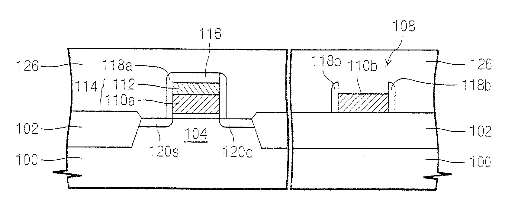
[0031] Referring to FIGS. 7A and 7B, a semiconductor device having a resistor pattern in accordance with this embodiment of the present invention includes a device isolation layer 102...


PUM


Abstract

Disclosed is a semiconductor device with a resistor pattern and methods of fabricating the same. Embodiments of the present invention provide a method of fabricating a resistor pattern having high sheet resistance by using a polycide layer for a gate electrode in a semiconductor device with the resistor pattern. Embodiments of the invention also provide a semiconductor device with a resistor pattern that is formed narrower than the minimum line width that can be defined in a photolithographic process so that sheet resistance thereof increases, and a method of fabricating the same.

Description

CROSS-REFERENCE TO RELATED APPLICATIONS [0001] This application is a Divisional of U.S. patent application Ser. No. 10 / 675,336, filed on Sep. 29, 2003, now pending, which claims priority from Korean Patent Application No. 2002-61403, filed on Oct. 9, 2002, the contents of which are herein incorporated by reference in their entirety.FIELD OF THE INVENTION [0002] This disclosure generally relates to semiconductor memory devices and, more specifically, to a semiconductor memory device with a resistor pattern and methods of fabricating the same. BACKGROUND OF THE INVENTION [0003] Semiconductor integrated circuits can be formed from active devices, such as diodes or transistors, and from passive devices such as capacitors, resistors, and inductors, in any combination. Typical integrated circuits use a resistor pattern having high resistance. Conventionally, the resistor pattern of a semiconductor device is formed of doped polysilicon having a relatively high sheet resistivity (Rs). The p...

Claims


Application Information

Patent Timeline
Patent Type & Authority Applications(United States)
IPC IPC(8): H01L21/8234H01L21/8246H01L27/02H01L21/8247H01L27/06H01L27/108H01L27/115
CPCH01L27/0629H01L27/10897H01L27/115Y10S257/904H01L27/11568H01L28/20H01L27/11531H10B12/50H10B69/00H10B41/42H10B43/30H01L27/02
Inventor SHIN, YOO-CHEOL
Owner SAMSUNG ELECTRONICS CO LTD
Why Eureka
Try Eureka