Methods of forming silicide layer of semiconductor device

a technology of semiconductor devices and silicide layers, which is applied in the direction of semiconductor devices, basic electric elements, electrical appliances, etc., can solve the problems of reducing the operation speed of the gate, deteriorating the operation speed of the device, and reducing the area of the unit device, so as to achieve the effect of increasing the sheet resistance of the ga

Inactive Publication Date: 2005-06-30
DONGBU ELECTRONICS CO LTD
View PDF5 Cites 7 Cited by
  • Summary
  • Abstract
  • Description
  • Claims
  • Application Information

AI Technical Summary

Benefits of technology

[0016] An object of the present invention is to provide a method of obviating an increase in the sheet resistance of a gate due to the reduction of a gate line-width.

Problems solved by technology

Such reduction in width increases the contact resistance of impurity regions as well as the sheet resistance of the gate, thereby deteriorating the operation speed of a device.
As described above, as a design rule for semiconductor devices becomes stricter, high sheet resistance of a gate reduces the operation speed of a device.
However, as a semiconductor device is highly integrated and the area of a unit device is reduced, forming sicilice with lower resistance is required.
However, the silicide made of metal and silicon is considerably thick and may not have a uniform thickness.
Generally, pure metal violently reacts with silicon to form silicide with rough interface morphology, which makes it difficult to accurately pattern a gate electrode in a later unit process.
In addition, uniform silcide may not be formed because of the dopant of high concentration in the polysilicon which reacts with the metal.
However, the method may generate particles during silicide formation.
In other words, because in the composite target consisting of metal and silicon the sputtering rate of the metal and the silicon is different each other, non-uniform silicide is formed, thereby generating particles.
However, the above-described conventional process of forming silicide layers has a problem that the sheet resistance of a gate increases because the width of a silicide layer formed on a gate is considerably reduced as the line-width of the gate is scaled down to less than a micron unit, thereby deteriorating the reliability of a device.

Method used


Image

  • Methods of forming silicide layer of semiconductor device
  • Methods of forming silicide layer of semiconductor device
  • Methods of forming silicide layer of semiconductor device

Examples


Embodiment Construction

[0022] Reference will now be made in detail to the preferred embodiments of the present invention, examples of which are illustrated in the accompanying drawings.

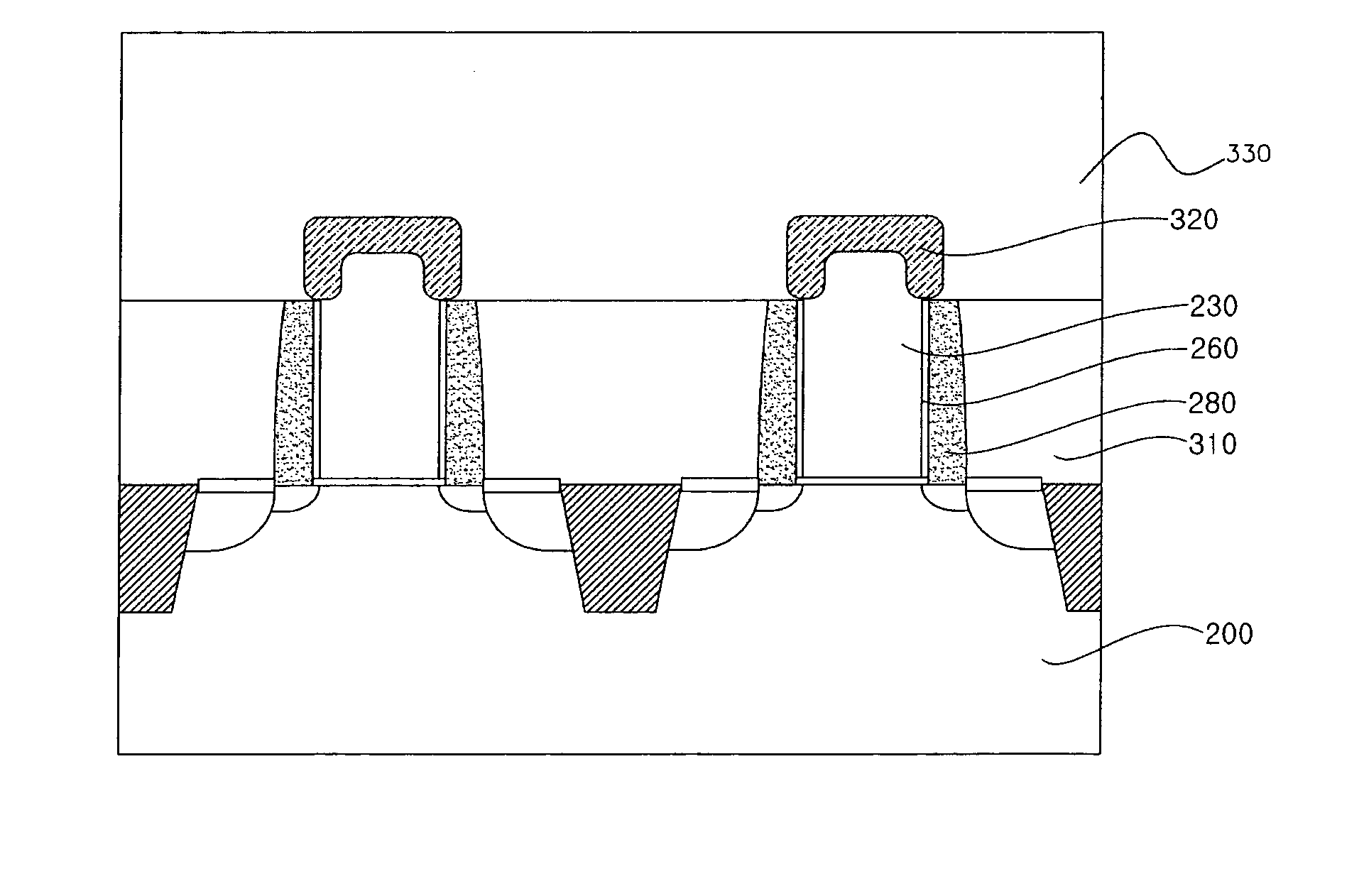
[0023]FIGS. 2a through 2e are cross-sectional views illustrating an example process of forming silicide layers of a semiconductor device.

[0024] Referring to FIG. 2a, at least one device isolation layer 210 is formed in a semiconductor substrate 200 by a shallow trench isolation process or a LOCOS process. A gate oxide layer 220 is formed on the semiconductor substrate 200. A polysilicon layer for a gate 230, a buffer oxide layer 240, and a buffer nitride layer 250 are sequentially deposited on the gate oxide layer 220. Some portion of the polysilicon layer, the buffer oxide layer, and the buffer nitride layer is removed to form a gate 230. A polyoxide layer 260 is formed on the sidewalls of the gate 230. An ion implantation process is performed to form LDD structures 270 in the semiconductor substrate 200. After an insula...


PUM


Abstract

Methods of forming silicide layers of a semiconductor device are disclosed. A disclosed method comprises depositing a polysilicon layer, a buffer oxide layer, and a buffer nitride layer on a semiconductor substrate; forming a gate on the semiconductor substrate by removing some portion of the polysilicon layer, the buffer oxide layer, and the buffer nitride layer; forming sidewall spacers on the sidewalls of the gate; forming source and drain regions in the semiconductor substrate by performing an ion implantation process; forming a first silicide layer on the source and drain regions; depositing a first ILD layer over the semiconductor substrate including the gate and the first silicide layer; removing some portion of the first ILD layer to expose the top surface of the gate; and forming a second silicide layer on the gate.

Description

FIELD OF THE INVENTION [0001] The present invention generally relates to semiconductor devices and, more particularly, to methods of forming silicide layers of a semiconductor device. BACKGROUND [0002] As semiconductor devices are highly integrated, the width of a gate and impurity regions that are used as source and drain regions are reduced. Such reduction in width increases the contact resistance of impurity regions as well as the sheet resistance of the gate, thereby deteriorating the operation speed of a device. [0003] To solve these problems, a method of forming interconnects of aluminum alloy or tungsten and a method of forming a silicide layer on a polysilicon gate have been suggested. Particularly, when a silicide layer is formed on a polysilicon gate, another silicide layer may be simultaneously formed on impurity regions to reduce the contact resistance of impurity regions. [0004] As described above, as a design rule for semiconductor devices becomes stricter, high sheet ...

Claims


Application Information

Patent Timeline
Patent Type & Authority Applications(United States)
IPC IPC(8): H01L21/28H01L21/24H01L21/336H01L21/8234
CPCH01L21/28044H01L29/6656H01L21/823443H01L21/28114H01L21/24
Inventor JUNG, JIN HYO
Owner DONGBU ELECTRONICS CO LTD
Why Eureka
Try Eureka