Multiple inlet atomic layer deposition reactor

a technology of atomic layer deposition reactor and multi-inlet, which is applied in the direction of chemical vapor deposition coating, coating, coating process, etc., can solve the problems of complex reactant flow, difficult rapid switching of reactant gases, and inconvenient design of conventional reactor designed for cvd

Inactive Publication Date: 2006-11-09
ASM GENITECH KOREA
View PDF24 Cites 76 Cited by
  • Summary
  • Abstract
  • Description
  • Claims
  • Application Information

AI Technical Summary

Benefits of technology

[0007] A conventional reactor designed for CVD is not suitable for efficient ALD because such a reactor is designed to simultaneously introduce reactants into its reaction chamber. In addition, in a reactor in which a reactant is introduced downward over a semiconductor substrate, a showerhead is typically used between a reactant inlet and the substrate to provide an evenly distributed flow over the substrate. Such a configuration, however, complicates the reactant flow and requires a large size reactor, making rapid switching of reactant gases difficult. Accordingly, there is a need to provide a reactor suitable for ALD, which allows prompt switching of one reactant to another while forming a high quality thin film.
[0007] A conventional reactor designed for CVD is not suitable for efficient ALD because such a reactor is designed to simultaneously introduce reactants into its reaction chamber. In addition, in a reactor in which a reactant is introduced downward over a semiconductor substrate, a showerhead is typically used between a reactant inlet and the substrate to provide an evenly distributed flow over the substrate. Such a configuration, however, complicates the reactant flow and requires a large size reactor, making rapid switching of reactant gases difficult. Accordingly, there is a need to provide a reactor suitable for ALD, which allows prompt switching of one reactant to another while forming a high quality thin film.
[0008] One aspect of the invention provides an atomic layer deposition reactor. The reactor comprises: a reaction chamber comprising a reaction space; a plurality of inlets; an exhaust outlet; and a gas flow control guide structure. The gas flow control guide structure resides over the reaction space. The gas flow control guide structure is interposed between the plurality of inlets and the reaction space. The gas flow control guide structure comprises a plurality of channels. Each of the plurality of channels extends from a respective one of the plurality of inlets to a first portion of a periphery of the reaction space. Each of the plurality of channels widens as the channel extends from the inlet to the reaction space. The reactor also includes a substrate holder positioned to expose a supported substrate to the reaction space.
[0009] Another aspect of the invention provides an atomic layer deposition (ALD) reactor. The reactor comprises: a reactor cover comprising a plurality of inlets and an exhaust outlet. The reactor also includes a reactor base comprising a substrate holder. The reactor base and the reactor cover are configured to define a reaction chamber. The reaction chamber comprises a reaction space. The reaction space comprises an upstream periphery and a downstream periphery positioned on the opposite side from the upstream periphery. The reactor further comprises a plurality of gas flow control plates positioned within the reactor chamber. The plurality of gas flow control plates reside over the reaction space. The plurality of gas flow control plates are stacked over one another. Each of the plurality of gas flow control plates at least partially defines an inflow channel configured to guide a reactant supplied through one of the plurality of the inlets to the upstream periphery of the reaction space.
[0010] Yet another aspect of the invention provides a method of depositing a reactant on a substrate in a reaction space. The reaction space comprises an upstream periphery and a downstream periphery. The method comprises a plurality of atomic layer deposition cycles, and each comprises: supplying a first reactant to the reaction space; reacting the first reactant with a surface of the substrate; removing excess first reactant from the reaction space; supplying a second reactant to the reaction space; reacting the second reactant with the surface of the substrate; and removing excess second reactant from the reaction space. Supplying the first reactant comprises in sequence: flowing the first reactant outwardly and horizontally at a first vertical level toward the upstream periphery of the reaction space while widening a first flow path of the first reactant, and flowing the first reactant vertically to the upstream periphery and into the reaction space. Supplying the second reactant comprises in sequence: flowing the second reactant horizontally at a second vertical level toward the upstream periphery of the reaction space while widening a second flow path of the second reactant, and flowing the second reactant vertically from the second vertical level to the upstream periphery and into the reaction space.
[0011] Yet another aspect of the invention provides a method of assembling an atomic layer deposition (ALD) reactor. In the method, a reactor cover is provided comprising a top plate and a sidewall. The top plate comprises a plurality of inlets, and defines an upper surface of a reaction chamber. The sidewall defines a side surface of the reaction chamber. The reaction chamber comprises a reaction space. Then, a gas flow control guide structure is placed into the reaction chamber so that at least a portion of the gas flow control guide structure is in contact with the upper surface of the reaction chamber. The gas flow control guide structure comprises a plurality of inflow channels. Each of the plurality of inflow channels extends from a respective one of the plurality of inlets to a first portion of a periphery of the reaction space. Next, a reactor base is provided to be in sealing contact with the sidewall of the reactor cover so that an upper surface of the reactor base and a lower surface of the gas flow control guide structure define the reaction space.

Problems solved by technology

A conventional reactor designed for CVD is not suitable for efficient ALD because such a reactor is designed to simultaneously introduce reactants into its reaction chamber.
Such a configuration, however, complicates the reactant flow and requires a large size reactor, making rapid switching of reactant gases difficult.

Method used


Image

  • Multiple inlet atomic layer deposition reactor
  • Multiple inlet atomic layer deposition reactor
  • Multiple inlet atomic layer deposition reactor

Examples


Embodiment Construction

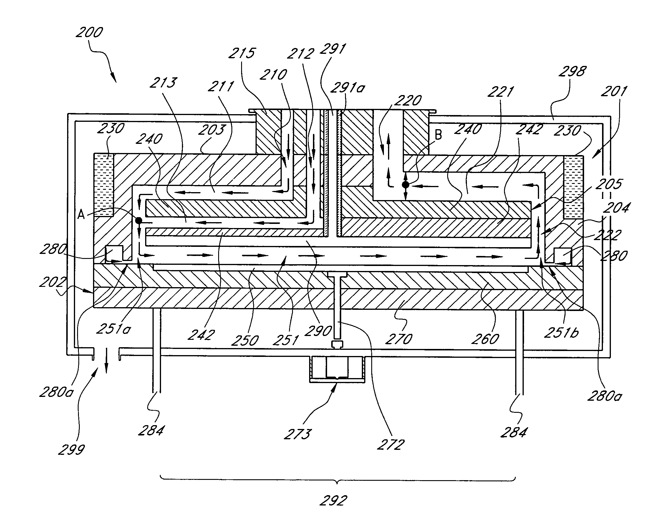
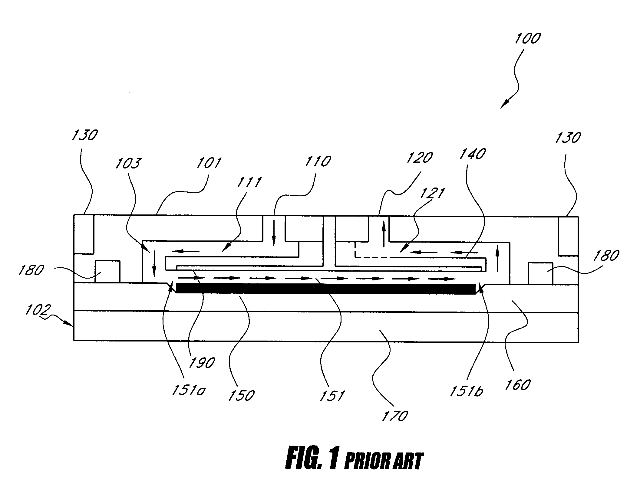
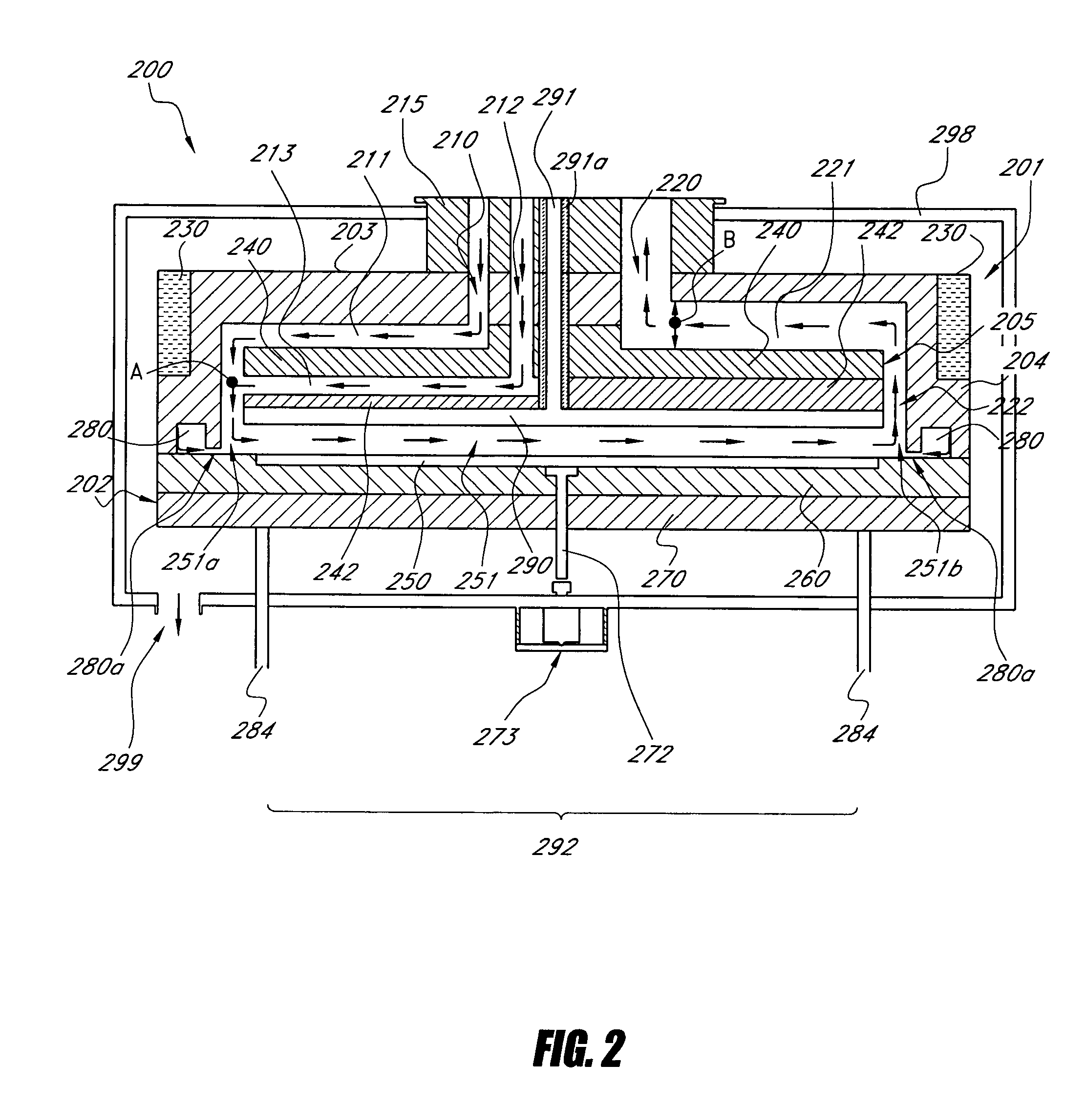
[0019]FIG. 1 illustrates an ALD reactor suitable for a sequential introduction of reactants into a reaction space, similar to that disclosed in U.S. Pat. No. 6,539,891. In FIG. 1, a reactor 100 includes a reactor cover 101, a reactor base 102, and a gas flow control plate 140.

[0020] The reactor cover 101 constitutes an upper part of the reactor 100, and has a short cylinder-like structure with its top blocked. The reactor cover 101 includes a reactant inlet 110 and an exhaust outlet 120. A portion of a side wall of the reactor cover 101 is surrounded by a cover heater 130.

[0021] The reactor base 102 is positioned below the reactor cover 101. The reactor base 102 can move vertically with respect to the reactor cover 101. A substrate 150 can be loaded or unloaded while the reactor base 102 is separated from the reactor cover 101. For deposition, the reactor base 102 moves up and is in sealing contact with the reactor cover 101. The reactor base 102 is configured to define a reaction...


PUM

PropertyMeasurementUnit
temperatureaaaaaaaaaa
cross-sectional areaaaaaaaaaaa

Abstract

A reactor configured to subject a substrate to alternately repeated surface reactions of vapor-phase reactants is disclosed. The reactor includes a reaction chamber, a plurality of inlets, and an exhaust outlet. The reaction chamber includes a reaction space. The reactor also includes a gas flow control guide structure within the reaction chamber. The gas flow control guide structure resides over the reaction space and is interposed between the plurality of inlets and the reaction space. The gas flow control guide structure includes a plurality of channels, and each of the channels extends from one of the inlets to an upstream periphery of the reaction space. Each of the channels progressively widens as the channel extends from the inlet to the reaction space. The reactor further includes a substrate holder in the reaction space.

Description

CROSS-REFERENCE TO RELATED APPLICATIONS [0001] This application claims the benefit of Korean Patent Application No. 2005-0038606, filed on May 9, 2005, in the Korean Intellectual Property Office, the disclosure of which is incorporated herein by reference. This application is also related to U.S. Pat. No. 6,539,891, issued on Apr. 1, 2003, entitled CHEMICAL DEPOSITION REACTOR AND METHOD OF FORMING A THIN FILM USING THE SAME, the disclosure of which is incorporated herein by reference.BACKGROUND OF THE INVENTION [0002] 1. Field of the Invention [0003] The present invention relates to an apparatus for growing thin films on a surface of a substrate. More particularly, the present invention relates to an apparatus for producing thin films on a surface of a substrate by subjecting the substrate to alternately repeated surface reactions of vapor-phase reactants. [0004] 2. Description of the Related Art [0005] In manufacturing semiconductor devices, various methods and apparatuses have bee...

Claims


Application Information

Patent Timeline
Patent Type & Authority Applications(United States)
IPC IPC(8): C23C16/00
CPCC23C16/4412C23C16/45519C23C16/5096C23C16/45548C23C16/45591C23C16/4554H01L21/10
Inventor KIM, DAEYOUNLEE, JEONG HOYOO, YONG MIN
Owner ASM GENITECH KOREA
Why Eureka
Try Eureka