Molding assembly for forming ingot and a method of forming ingot

a molding assembly and ingot technology, applied in the direction of moulding machines, crystal growth processes, chemically reactive gases, etc., can solve the problems of high cost of manufacturing the substrate, wear of the molding device, and difficulty in recycling the molding devi

Inactive Publication Date: 2006-11-09
KYOCERA CORP
View PDF2 Cites 14 Cited by
  • Summary
  • Abstract
  • Description
  • Claims
  • Application Information

AI Technical Summary

Benefits of technology

The present invention is related to a molding assembly for forming an ingot. The assembly includes side members and a bottom member. The side members have engaging end portions that are engaged with each other to form a polygonal prism with sides, corners, a top opening, and a bottom opening. The bottom member is fitted to close the bottom opening of the prism to form a molding device for molding a molten material into an ingot. The technical effect of this invention is to provide a more efficient and precise method for forming ingots of molten materials.

Problems solved by technology

However, a cost of manufacturing the substrate is high.
In the molding device made of fused silica, during a process of cooling a block from the high-temperature state, the molding device is cracked due to the temperature gradient and difference of the sintering state inside the molding device, making it difficult to recycle the molding device.
Also, in the molding device made of the quartz, a surface layer of the inner surface of the molding device coated with the mold release material becomes cristobalite, and the surface layer is peeled, causing wearing of the molding device and making it extremely difficult to recycle.
Thus, the yield of the manufactured silicon ingots is poor.
Accordingly, the side surfaces of a silicon ingot cast by this molding device have an inverted taper expanding from the bottom of the ingot toward the top, thereby increasing edge portions which cannot be used as products.
Therefore, expensive raw silicon materials are removed excessively.

Method used


Image

  • Molding assembly for forming ingot and a method of forming ingot
  • Molding assembly for forming ingot and a method of forming ingot
  • Molding assembly for forming ingot and a method of forming ingot

Examples


example

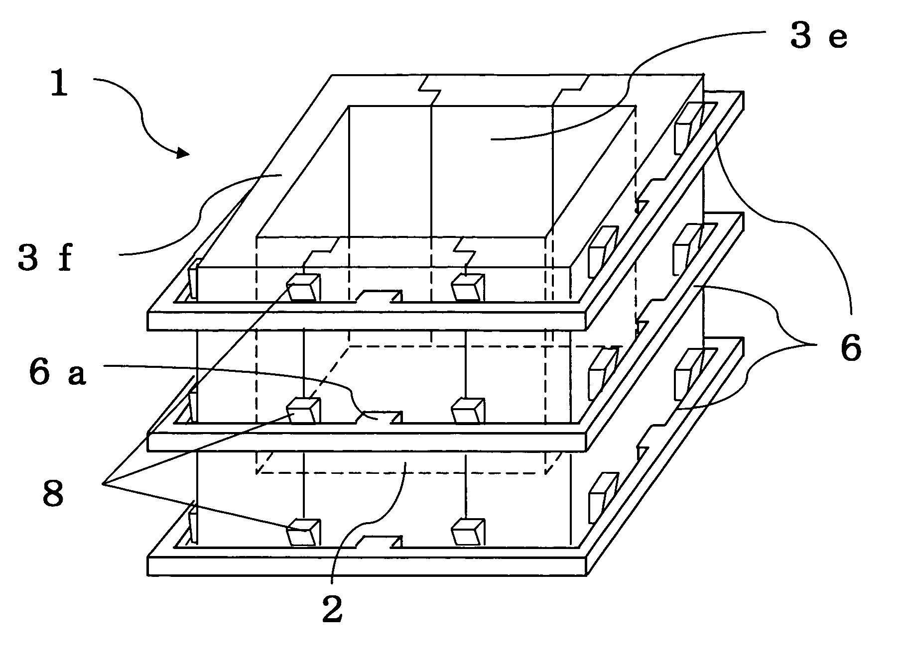
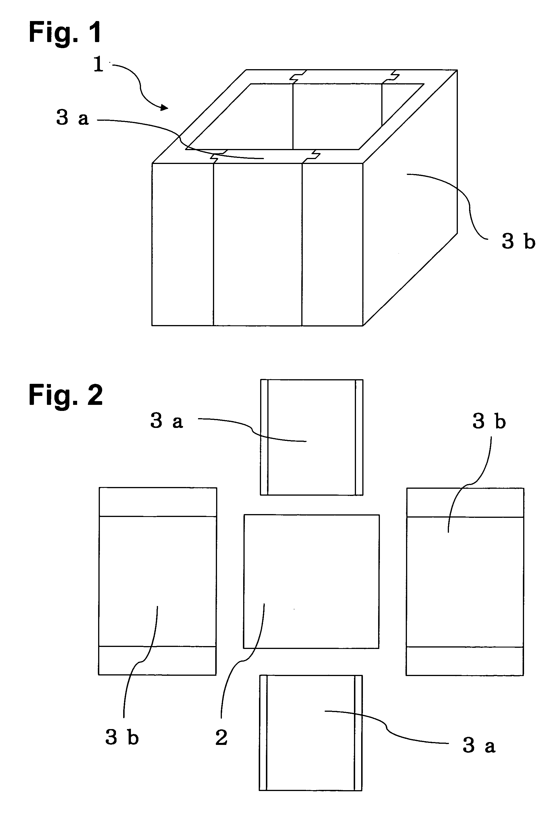
[0078] When a molding device assembled by using screws is compared with the molding device 1 according to the embodiment of the invention shown in FIG. 16, the following result may be expected.

[0079] A bottom member (20 mm in thickness) and four side members (20 mm in thickness), made of graphite and coated with a mold release material made of silicon nitride, may be assembled into a box shape, and fixed by forty screws (ø 5 mm x 40 mm in length), thereby obtaining a molding device (350 mm × 350 mm in inner dimension × 350 mm in height). Then, 90 kg of a molten silicon material is poured into the molding device obtained as described above, and by gradually decreasing a temperature of the molten silicon material from the bottom of the molding device, it is expected that a silicon ingot with 315 mm in height can be obtained.

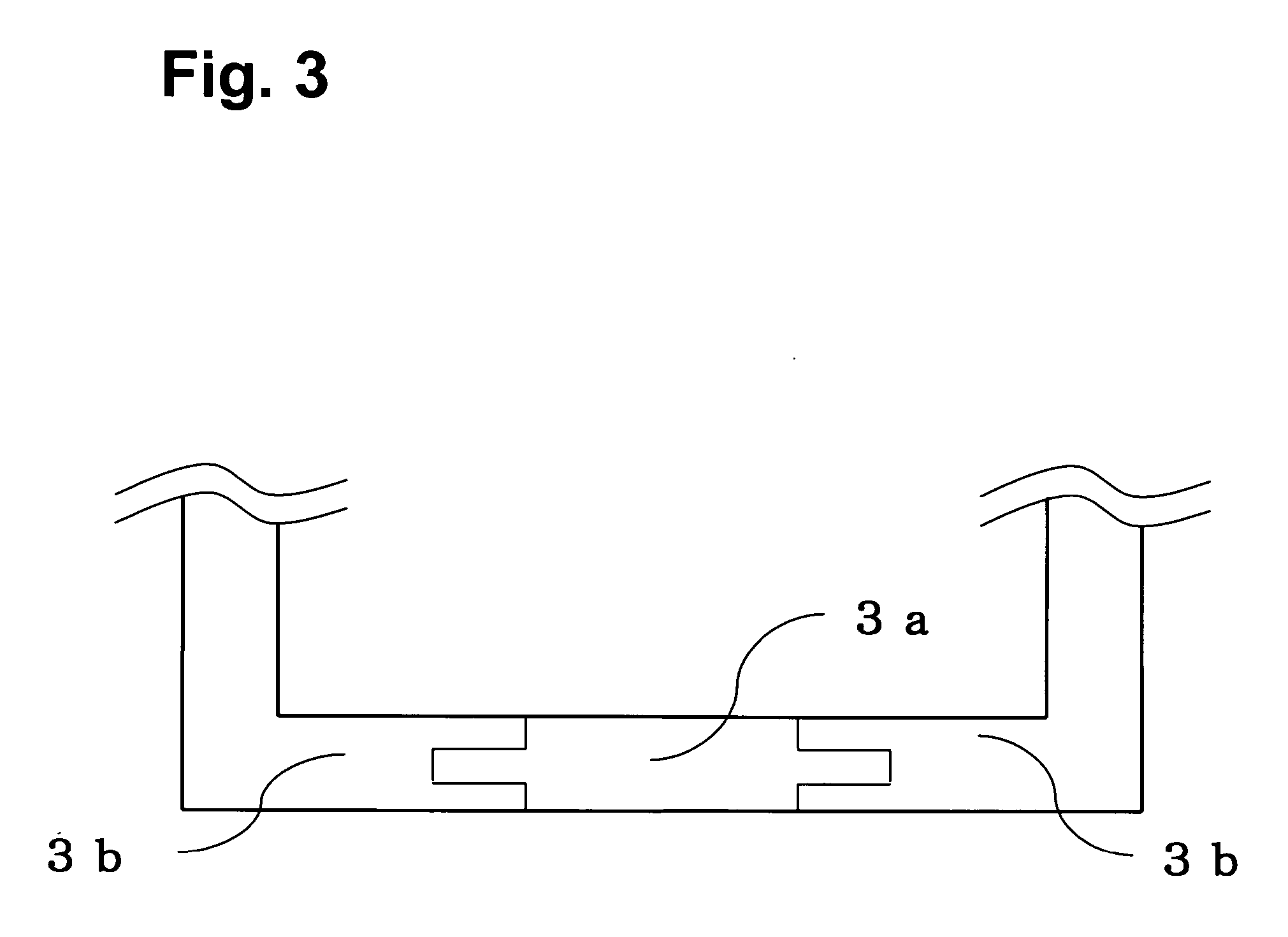
[0080] For the molding device according to the embodiment of the present invention as shown in FIG. 16, the bottom member 2 (10 mm in thickness), two first side ...


PUM

PropertyMeasurementUnit
lengthaaaaaaaaaa
densityaaaaaaaaaa
densityaaaaaaaaaa

Abstract

A molding assembly for forming an ingot, including side members each having engaging end portions, the engaging end portions of the side members being engaged with respective ones of the side members such that the side members form a polygonal prism having sides, corners, a top opening and a bottom opening, the engaging end portions of the side members engaging to form connecting portions positioned in the sides, and a bottom member fitted to close the bottom opening of the polygonal prism so as to form a molding device for molding a molten material into an ingot.

Description

CROSS-REFERENCE TO RELATED APPLICATIONS [0001] The present application claims priority to Japanese Patent Application Serial No. 2005-134936, filed on May 6, 2005. The contents of that application are incorporated herein by reference in their entirety. BACKGROUND OF THE INVENTION [0002] 1. Field of the Invention [0003] The present invention relates to a molding device for forming an ingot from a molten material, and a method of forming an ingot from a molten material. [0004] 2. Discussion of the Background [0005] As a clean energy source alternative to petroleum oil, practical use of solar batteries has been sought in an extensive field ranging from a small-scaled house hold use to a large-scaled power generation system. These solar batteries are classified into a crystal type, an amorphous type, and a compound type in accordance with types of materials used, and among them, a majority of the solar batteries currently distributed in the market are crystal type silicon solar batterie...

Claims


Application Information

Patent Timeline
Patent Type & Authority Applications(United States)
IPC IPC(8): A01J25/13
CPCB22D7/06Y10T117/1092C30B11/002C01B33/02
Inventor ATOBE, JUNICHI
Owner KYOCERA CORP
Why Eureka
Try Eureka