Module,filter, and antenna technology millimeter waves multi-gigabits wireless systems

a filter and antenna technology, applied in the field of communication networks, can solve the problems of high cost of mmic (monolithic microwave integrated circuit) chipsets and packaging devices operating at ultra-high frequencies and/or ultra-high speeds, affecting the number of consumers, and mmw radios are often expensive many hundred, or even several thousand dollars, and achieve accurate alignment

Active Publication Date: 2006-11-09
GEORGIA TECH RES CORP
View PDF16 Cites 26 Cited by
  • Summary
  • Abstract
  • Description
  • Claims
  • Application Information

AI Technical Summary

Benefits of technology

[0019] In a preferred embodiment, the adhesive is a pressure sensitive adhesive enabling room-temperature lamination, a solid electrical connection between connections, and an accurate alignment of the top layer and the bottom layer.

Problems solved by technology

Unfortunately, the high cost of MMIC (monolithic microwave integrated circuit) chipsets and packaging devices operating at ultra-high frequencies and / or ultra-high speeds affects the number of consumers that can enjoy these advances in technology.
Conventional solutions of MMW radios cost often several hundred, or even several thousand dollars.
The high costs of MMW radios are due to high costs of material used, as well as costs associated with low volume fabrication, and assembly processes.
Moreover, antennas for MMW radios are traditionally implemented using either metallic horn antennas, or large planar array printed micro-strips, that are connected to a module, which further increase manufacturing costs.

Method used


Image

  • Module,filter, and antenna technology millimeter waves multi-gigabits wireless systems
  • Module,filter, and antenna technology millimeter waves multi-gigabits wireless systems
  • Module,filter, and antenna technology millimeter waves multi-gigabits wireless systems

Examples


Embodiment Construction

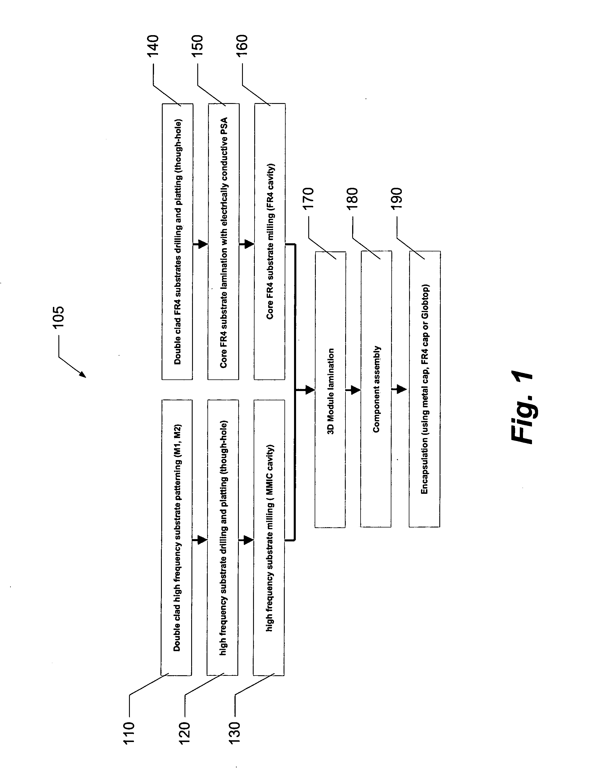
[0060] To facilitate an understanding of the principles and features of the invention, it is explained hereinafter with reference to its implementation in an illustrative embodiment. In particular, the invention is described in the context of being a wireless module for operation at ultra-high frequencies and ultra-high data communication speeds.

[0061] The materials described as making up the various elements of the invention are intended to be illustrative and not restrictive. Many suitable materials that would perform the same or a similar function as the materials described herein are intended to be embraced within the scope of the invention. Such other materials not described herein can include, but are not limited to, for example, materials that are developed after the time of the development of the invention.

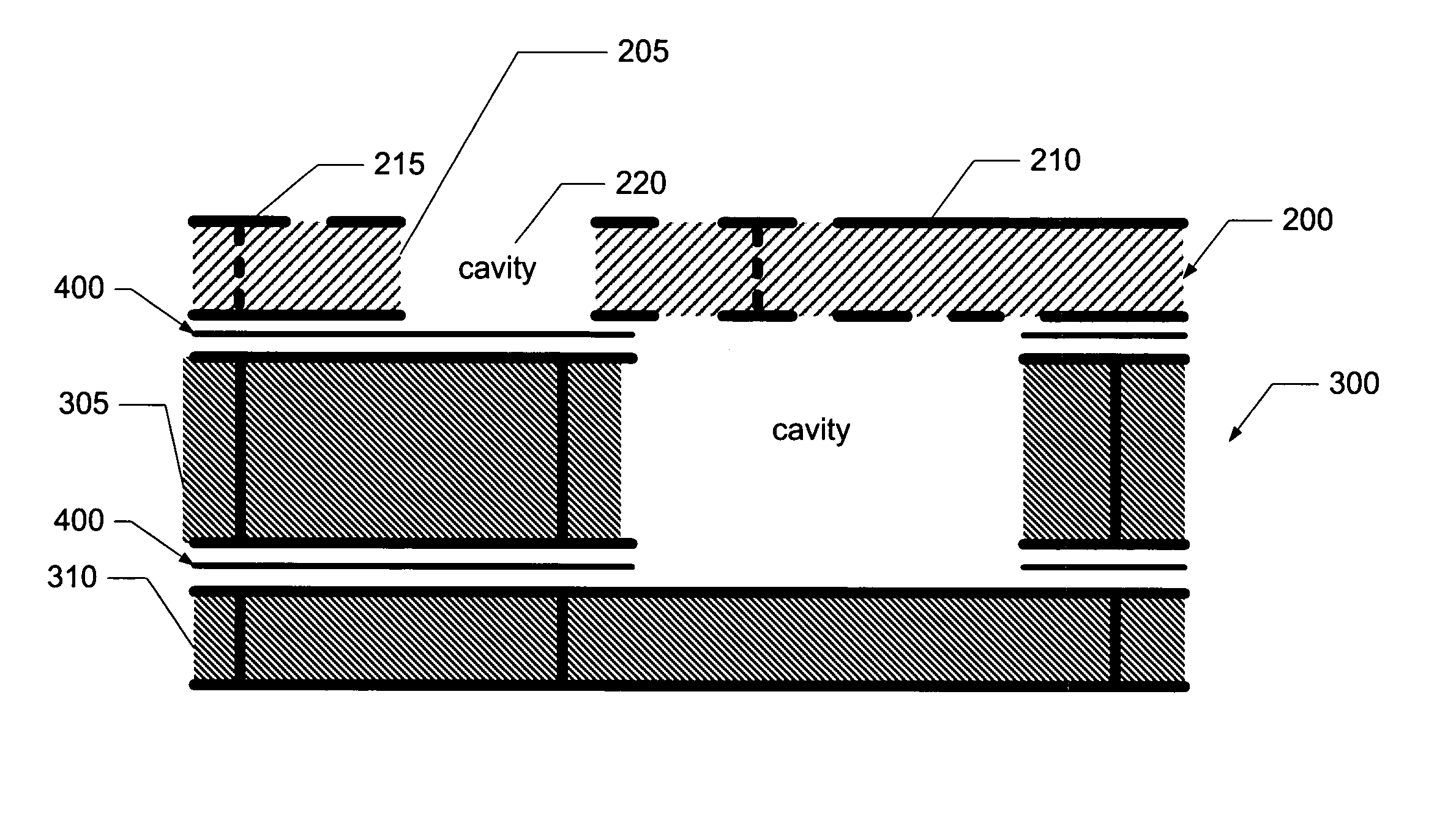
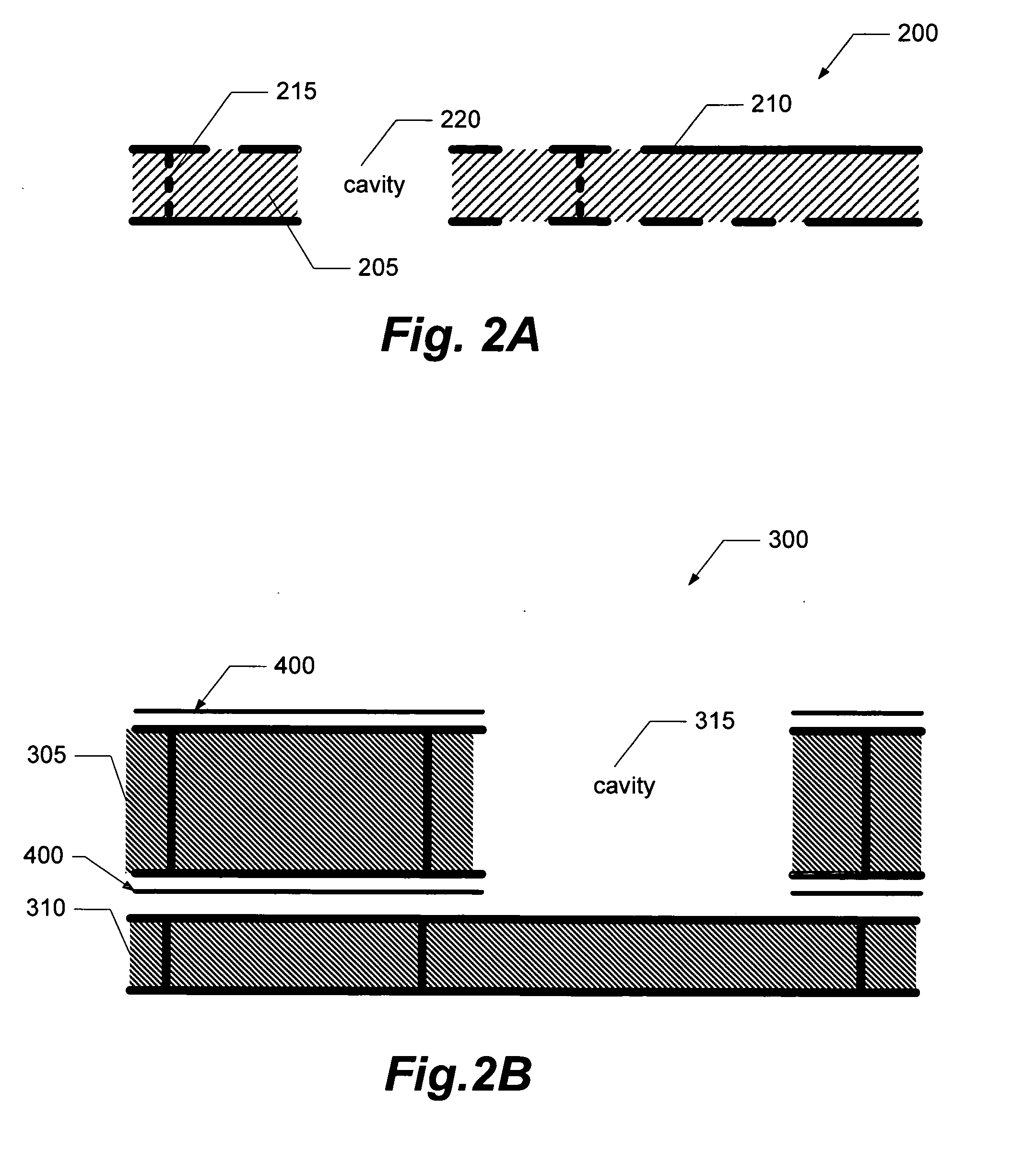
[0062] The present invention is a wireless module 100. The module 100 preferably includes a top layer 200, a bottom layer 300, and an adhesive 400 to connect the top lay...


PUM

PropertyMeasurementUnit
frequencyaaaaaaaaaa
thicknessaaaaaaaaaa
thicknessaaaaaaaaaa

Abstract

A method of fabricating an ultra-high frequency module is disclosed. The method includes providing a top layer; drilling the top layer; milling the top layer; providing a bottom; milling the bottom layer to define a bottom layer cavity; aligning the top layer and the bottom layer; and adhering the top layer to the bottom layer. The present invention also includes an ultra-high frequency module operating at ultra-high speeds having a top layer, the top layer defining a top layer cavity; a bottom layer, the bottom layer defining a bottom layer cavity; and an adhesive adhering both the top layer to the bottom layer, wherein the top layer and the bottom layer are formed from a large area panel of a printed circuit board.

Description

CROSS-REFERENCE TO RELATED APPLICATIONS [0001] This application claims the benefit of U.S. Provisional Application Nos. 60 / 666,839 and 60 / 666,840, both filed 31 Mar. 2005, and U.S. Provisional Application Nos. 60 / 667,287, 60 / 667,312, 60 / 667,313, 60 / 667,375, 60 / 667,443, and 60 / 667,458, collectively filed 1 Apr. 2005, the entire contents and substance of which are hereby incorporated by reference.BACKGROUND OF THE INVENTION [0002] 1. Field of the Invention [0003] The present invention relates to communication networks and, more particularly, to improved packaging of high speed communication devices. [0004] 2. Description of Related Art [0005] As the world becomes more reliant on electronic devices, and portable devices, the desire for faster and more convenient devices continues to increase. Accordingly, manufacturers and designers of such devices strive to create faster, easier to use, and more cost-effective devices to serve the needs of consumers. [0006] Indeed, the demand for ultr...

Claims


Application Information

Patent Timeline
Patent Type & Authority Applications(United States)
IPC IPC(8): H01Q9/04H01P1/203
CPCH01P1/20327Y10T29/4913H01P11/007H01P11/008H01Q1/38H01Q21/0006H01Q21/0087H01Q21/065H01Q21/08H01Q23/00Y10T29/49002Y10T29/49165Y10T156/10Y10T29/49016H01P1/2039
Inventor PINEL, STEPHANELASKAR, JOY
Owner GEORGIA TECH RES CORP
Why Eureka
Try Eureka