CAM device and method for repairing the same

Inactive Publication Date: 2006-11-16
SAMSUNG ELECTRONICS CO LTD
View PDF5 Cites 4 Cited by
  • Summary
  • Abstract
  • Description
  • Claims
  • Application Information

AI Technical Summary

Benefits of technology

[0027] Therefore, the present invention is directed to provide a content addressable memory (CAM) device and a method for repairing the CAM device, capable of addressing difficulties caused by the latch structure of a cell in a primary cell array.

Problems solved by technology

In a read / write operation or a search operation of the CAM device, specific defective ones of a plurality of CAM cells constituting the CAM device may cause an error.
Further, the defective cells may disable the operation of the CAM.
In the CAM device using the above-described repairing method, however, the defective entry participates in generating entry information at the primary encoder and unintended final entry information is output when search data match specific pattern data of the defective entry, due to a characteristic caused by a latch structure of a cell of a primary cell array, i.e., a characteristic of maintaining specific pattern data, even after substitution and repair into an entry in the redundant cell array so a defective entry does not participate in generating entry information.
However, as the CAM cell of the primary cell array is formed in a latch structure, the defective entry participates in generating entry information at the primary encoder, which causes an operation error in the CAM device.

Method used


Image

  • CAM device and method for repairing the same
  • CAM device and method for repairing the same
  • CAM device and method for repairing the same

Examples


Embodiment Construction

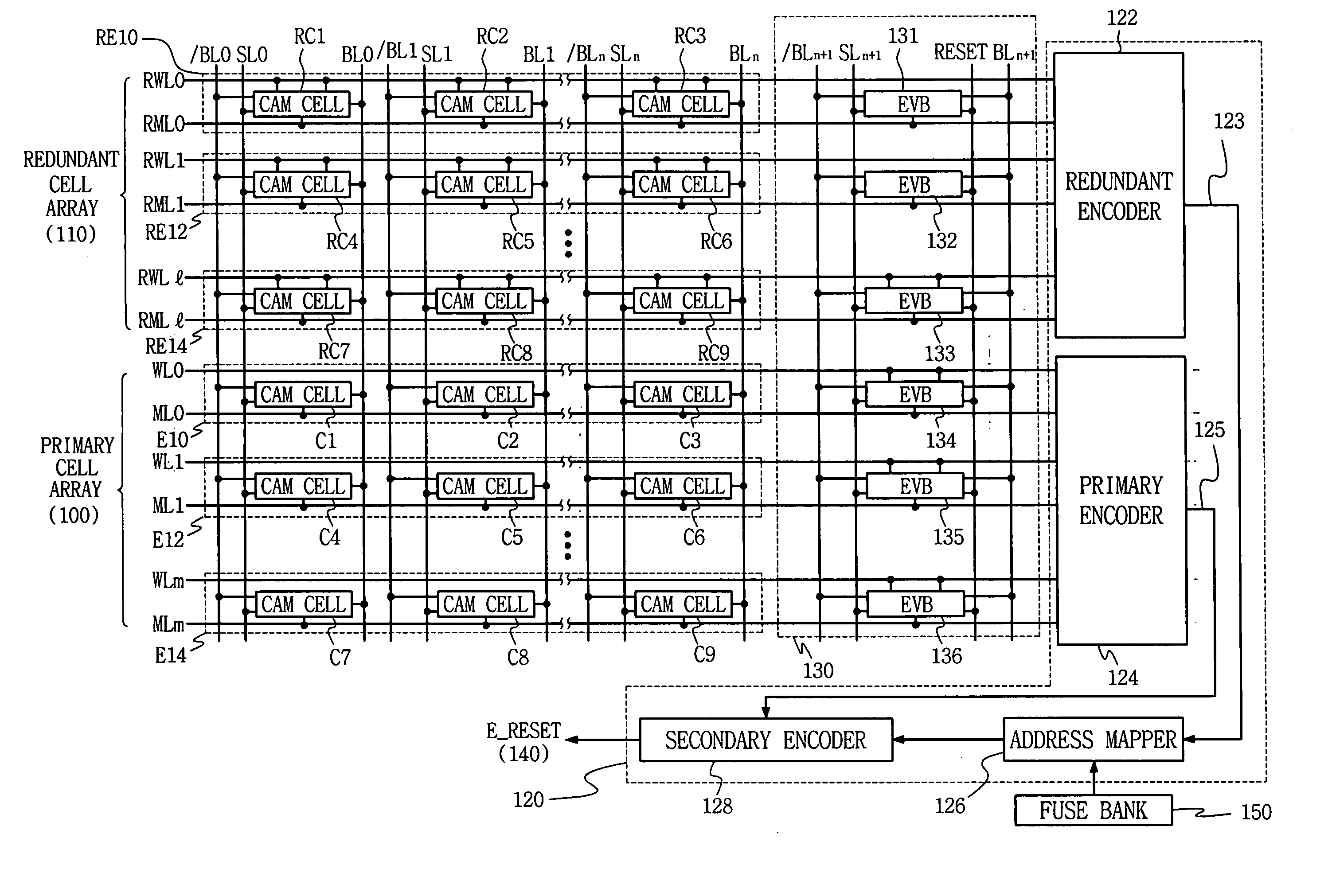
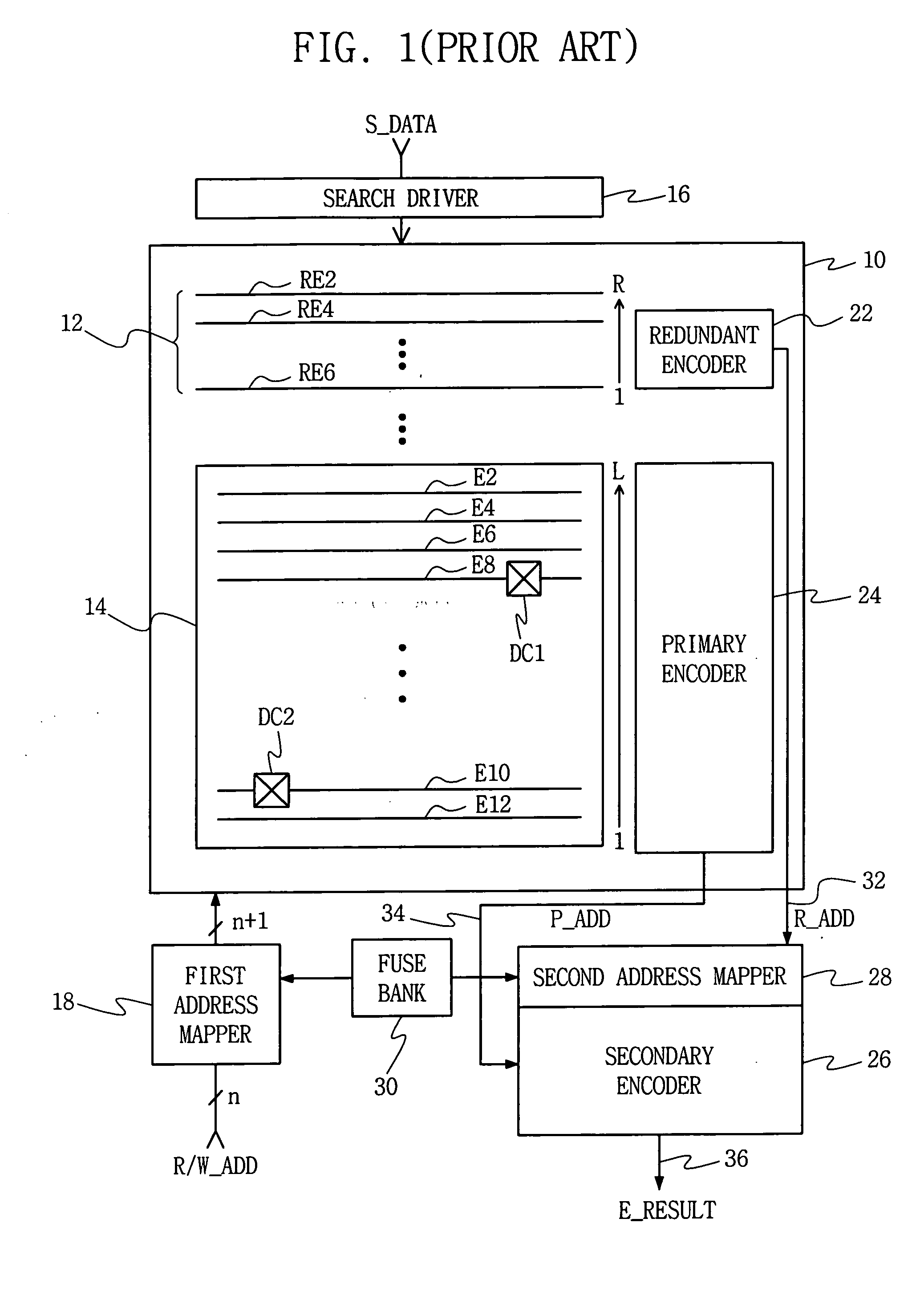
[0047] The present invention will now be described with reference to the accompanying drawings, in which exemplary embodiments of the invention are shown. However, the invention should not be construed as limited to the embodiments set forth herein. In the drawings, like numbers refer to like elements.

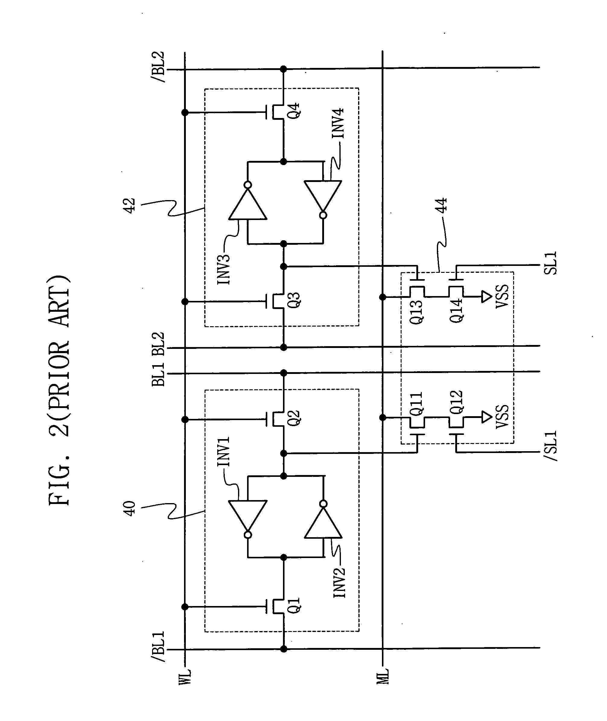
[0048]FIG. 2 is a circuit diagram illustrating a conventional ternary CAM cell. Since the ternary CAM cell in FIG. 2 may be an example of a CAM cell applied to the CAM device of the present invention, it will be described in greater detail.

[0049] Referring to FIG. 2, the ternary CAM cell includes SRAM cells 40 and 42 for storing data, and a comparing circuit 44.

[0050] The SRAM cell 40 includes a latch circuit including two inverters INV1 and INV2, and access transistors Q1 and Q2 each having a gate connected to a word line WL and transmitting data on bit lines BL1 and / BL1 to the latch.

[0051] Similarly, the SRAM cell 42 includes a latch circuit including two inverters INV3 and INV4...


PUM


Abstract

A content addressable memory (CAM) device is provided that includes a primary cell array having at least one entry in which a plurality of CAM cells are connected to word lines and match lines, a redundant cell array having entries formed in the same structure as that of the entries in the primary cell array to substitute for a defective entry including one or more defective CAM cells in the primary cell array, an encoder for receiving a match signal from an entry in the CAM array block having data matching search data to generate final entry information, and an entry controlling circuit for determining whether each entry in the CAM array block is used to generate the final entry information at the encoder, and inhibiting a signal applied from a match line of the defective entry from participating in generating the final entry information at the encoder.

Description

CROSS-REFERENCE TO RELATED APPLICATION [0001] This application claims the benefit of Korean Patent Application No. 10-2005-0038783, filed May 10, 2005, the disclosure of which is incorporated by reference herein in its entirety. BACKGROUND OF THE INVENTION [0002] 1. Technical Field [0003] The present invention relates to semiconductor memory devices, and more particularly, to a content addressable memory (CAM) device and a method for repairing the CAM device. [0004] 2. Discussion of Related Art [0005] In a random access memory (RAM) or a read only memory (ROM), an address is input to read data that is stored in a memory cell designated by the address. However, in a content addressable memory (CAM) device, external data is received and compared to stored data to determine whether it matches the stored data, and a signal corresponding to the comparing result is output. The signal corresponding to the comparing result may be in an address, pointer, or bit pattern form, which is referre...

Claims


Application Information

Patent Timeline
IPC IPC(8): G11C15/00
CPCG11C15/04G11C5/063G11C8/08G11C29/70
Inventor LEE, IN-YOUL
Owner SAMSUNG ELECTRONICS CO LTD
Why Eureka
Try Eureka