Substrate processing and method of manufacturing device

a technology of substrate and manufacturing device, which is applied in the direction of coating, magnetic-bias transformer, chemical vapor deposition coating, etc., can solve the problem of physical damage of substra

Inactive Publication Date: 2006-11-23
KOKUSA ELECTRIC CO LTD
View PDF8 Cites 27 Cited by
  • Summary
  • Abstract
  • Description
  • Claims
  • Application Information

AI Technical Summary

Benefits of technology

[0025] an isolation transformer having a primary side coil which is electrically connected to said hi...

Problems solved by technology

The high energy ion charges up a circuit element which has already been produced on the substrate, the high energy ion destroys the circuit element, and if...

Method used


Image

  • Substrate processing and method of manufacturing device
  • Substrate processing and method of manufacturing device
  • Substrate processing and method of manufacturing device

Examples


second embodiment

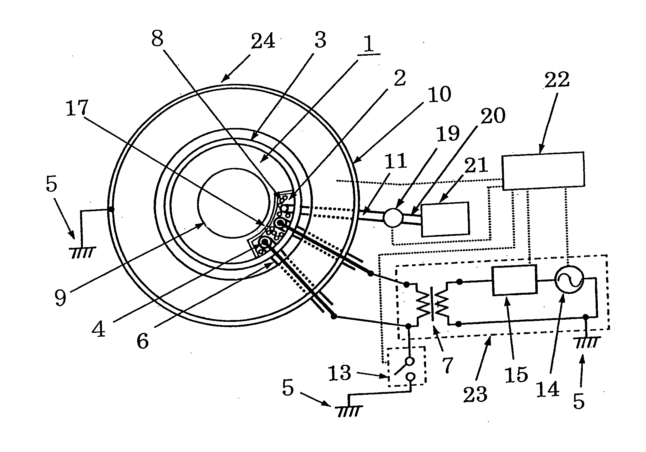
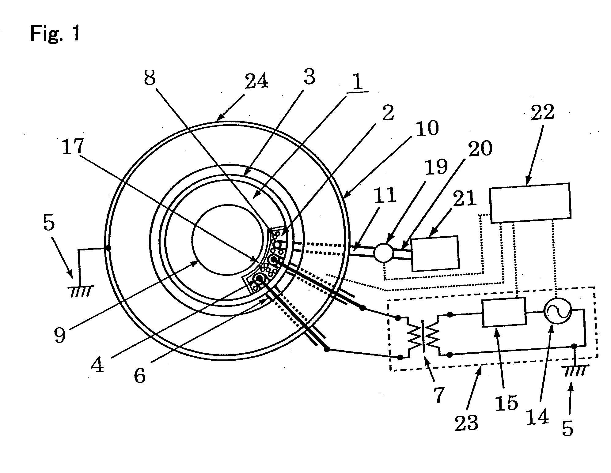
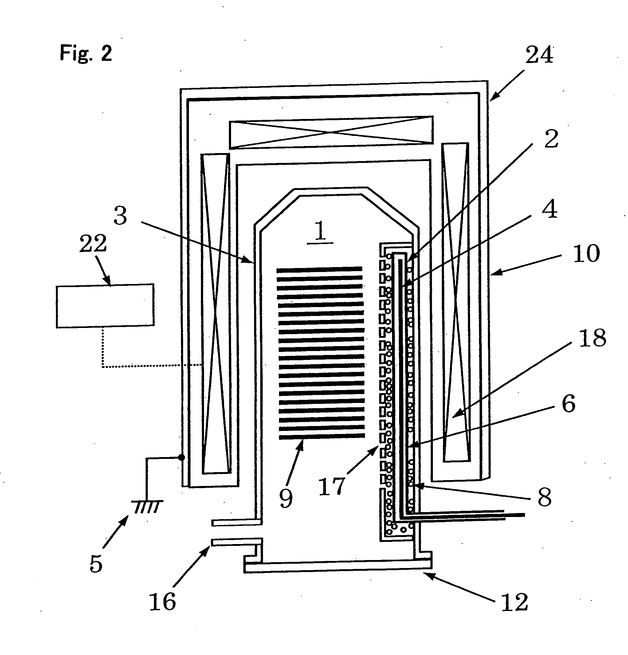
[0079]FIGS. 3 and 5 are schematic transverse sectional views and FIGS. 4 and 6 are schematic vertical sectional views of the processing furnace 24 of the vertical decompression CVD apparatus of the present invention.

[0080] The second embodiment shown in FIGS. 3 to 6 is different from the first embodiment shown in FIGS. 1 and 2 in that one end of a supply line connected to the electrodes 4 of the isolation transformer 7 is connected to the ground 5, and the control unit 22 controls the opening and closing operation of the switch 13. The switch 13 may not be switched by the control unit 22 and may be switched manually.

[0081]FIGS. 3 and 4 show a state in which the switch 13 is opened, the electrodes 4 are insulated from the conductive members (e.g., the seal flange 12, the heater wire, the cover 10 and the like) around the processing chamber 1, and plasma 8 is produced only in the buffer chamber 2. FIGS. 5 and 6 show a state in which the electrodes 4 are connected to the conductive me...


PUM

PropertyMeasurementUnit
Thicknessaaaaaaaaaa
Electrical conductoraaaaaaaaaa
Frequencyaaaaaaaaaa

Abstract

A substrate processor enables realization of a proper process by combining advantages of a remote plasma and a plasma generated in an entire processing chamber. The substrate processor includes a conductive member (10) which is installed surrounding a processing space (1) and grounded to the earth and a pair of electrodes (4) installed inside the conductive member (10). A primary coil of an insularing transformer (7) is connected to a high-frequency power supply unit (14) and a secondary coil is connected to the electrodes (4). A switch (13) is connected to the connection line connecting the secondary coil to the electrodes (4). By setting up/cutting off the connection of the line to the earth with use of the switch (13), the region where the plasma is generated in the processing space (1) can be changed.

Description

TECHNICAL FIELD [0001] The present invention relates to a substrate processing apparatus and a producing method of a device, and more particularly, to a substrate processing apparatus which carries out processing such as forming a thin film on a substrate such as a wafer, impurity diffusion and etching, and to a producing method of a device using the substrate processing apparatus. BACKGROUND ART [0002] Some substrate processing apparatuses such as semiconductor producing apparatuses activate processing gas such as raw material gas used for processing a substrate, and carries out processing such as film formation on the substrate. [0003] If plasma is produced by discharging, electrically neutral radical (active species) having relatively long lifetime and small energy, and charged ion having relatively short lifetime and great energy are generated at the same time. A remote plasma type substrate processing apparatus produces plasma only in a buffer chamber (discharge chamber) isolat...

Claims


Application Information

Patent Timeline
IPC IPC(8): H01L21/44C23C16/00C23C16/50H01F19/08H01J37/32H01L21/00
CPCC23C16/50H01F19/08H01L21/67253H01J37/32174H01J37/32082H01L21/3065H01L21/02
Inventor TOYODA, KAZUYUKISHIMA, NOBUHITOISHIMARU, NOBUOKONNO, YOSHIKAZUTAKEBAYASHI, MOTONARINODA, TAKAAKIMIZUNO, NORIKAZU
Owner KOKUSA ELECTRIC CO LTD
Why Eureka
Try Eureka