Plasma processing apparatus and plasma processing method
a plasma processing and plasma technology, applied in the direction of electrical apparatus, electric discharge tubes, basic electric elements, etc., can solve the problems of preventing the performance of the processing from being varied with time, and achieve the effect of improving the yield of plasma processing and improving the reliability of the plasma processing apparatus
- Summary
- Abstract
- Description
- Claims
- Application Information
AI Technical Summary
Benefits of technology
Problems solved by technology
Method used
Image
Examples
first modification
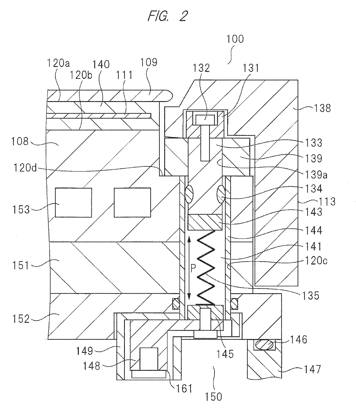
[0076]A first modification of this embodiment will be described with reference to FIG. 6. FIG. 6 is a schematic cross-sectional view illustrating, in enlarged dimension, the configuration of a susceptor ring portion of the sample stage of the plasma processing apparatus according to the first modification of the embodiment of the present invention.
[0077]In place of the plate spring 135 of the electric power supply connector 161 having the configuration in FIG. 2, the plasma etching apparatus 100 of the first modification includes a coil spring (spring member, conductive member) 154 including a conductive member, such as metal, and wound in a plurality of stages about the axis in the up-down direction P to have resiliency. The plasma etching apparatus 100 of the first modification includes the same configuration as the plasma etching apparatus 100 in FIG. 2 except for the coil spring 154. As the material of the coil spring 154, for example, austenitic SUS304-CSP is used, and to lower...
second modification
[0079]Another modification (second modification) of the first modification will be described with reference to FIGS. 7 and 8. FIG. 7 is a schematic cross-sectional view illustrating, in enlarged dimension, the configuration of a susceptor ring portion of the sample stage of the plasma processing apparatus according to the second modification of the embodiment of the present invention, and FIG. 8 is a schematic perspective view illustrating, in enlarged dimension, the configuration of a curved plate spring illustrated in FIG. 7.
[0080]In place of the plate spring 135 of the electric power supply connector 161 having the configuration in FIG. 2, the plasma etching apparatus 100 of the second modification includes a curved plate spring 142 including a plate member including a conductive member, such as metal, and having unevenness in a left-right direction R indicated in FIG. 8. The plasma etching apparatus 100 of the second modification includes the same configuration as the plasma etc...
third modification
[0082]A further modification (third modification) of the above embodiment will be described with reference to FIG. 9. FIG. 9 is a schematic cross-sectional view illustrating, in enlarged dimension, the configuration of a susceptor ring portion of the sample stage of the plasma processing apparatus according to the third modification of the embodiment of the present invention.
[0083]In place of the plate spring 135 of the electric power supply connector 161 having the configuration in FIG. 2, the plasma etching apparatus 100 of the third modification includes stranded wires (conductive members) 155 formed by stranding a plurality of conductive wires that are conductive members, such as metal (for example, electric power supply wires). The plasma etching apparatus 100 of the third modification includes the same configuration as the plasma etching apparatus 100 in FIG. 2 except for the stranded wires 155. In the third modification, as the material of the stranded wires 155, for example,...
PUM
 Abstract
Description
Claims
Application Information


