Optical transmitting apparatus, optical receiving apparatus, and optical communication system comprising them

a technology of optical transmission apparatus and optical receiving apparatus, which is applied in the direction of transmission monitoring/testing/fault-measurement system, electrical apparatus, instruments, etc., can solve the problem that no measures have been taken to prevent the loss of accuracy of optical devices, and achieve the effect of stabilizing the quality of output optical signals and eliminating the deterioration of receiving characteristics

Active Publication Date: 2006-11-23
FUJITSU LTD
View PDF26 Cites 139 Cited by
  • Summary
  • Abstract
  • Description
  • Claims
  • Application Information

AI Technical Summary

Benefits of technology

[0018] According to the present invention, quality of the output optical signal can be stabilized by controlling phase shift, which may deviate by fluctuation of temperature change or aging and so forth of components constituting an optical tr

Problems solved by technology

The ABC circuit in the conventional optical transmitting apparatus employing the NRZ modulation, however, only performs bias control, which compensates for the deviation of an operating point of the MZ modulator, and it does not comprise means for monitoring the amount of phase shift of a phase shift unit necessary for phase shift keying such as DQPSK, which is receiving attention for its anticipated potential.
There was a problem t

Method used


Image

  • Optical transmitting apparatus, optical receiving apparatus, and optical communication system comprising them
  • Optical transmitting apparatus, optical receiving apparatus, and optical communication system comprising them
  • Optical transmitting apparatus, optical receiving apparatus, and optical communication system comprising them

Examples


tenth embodiment

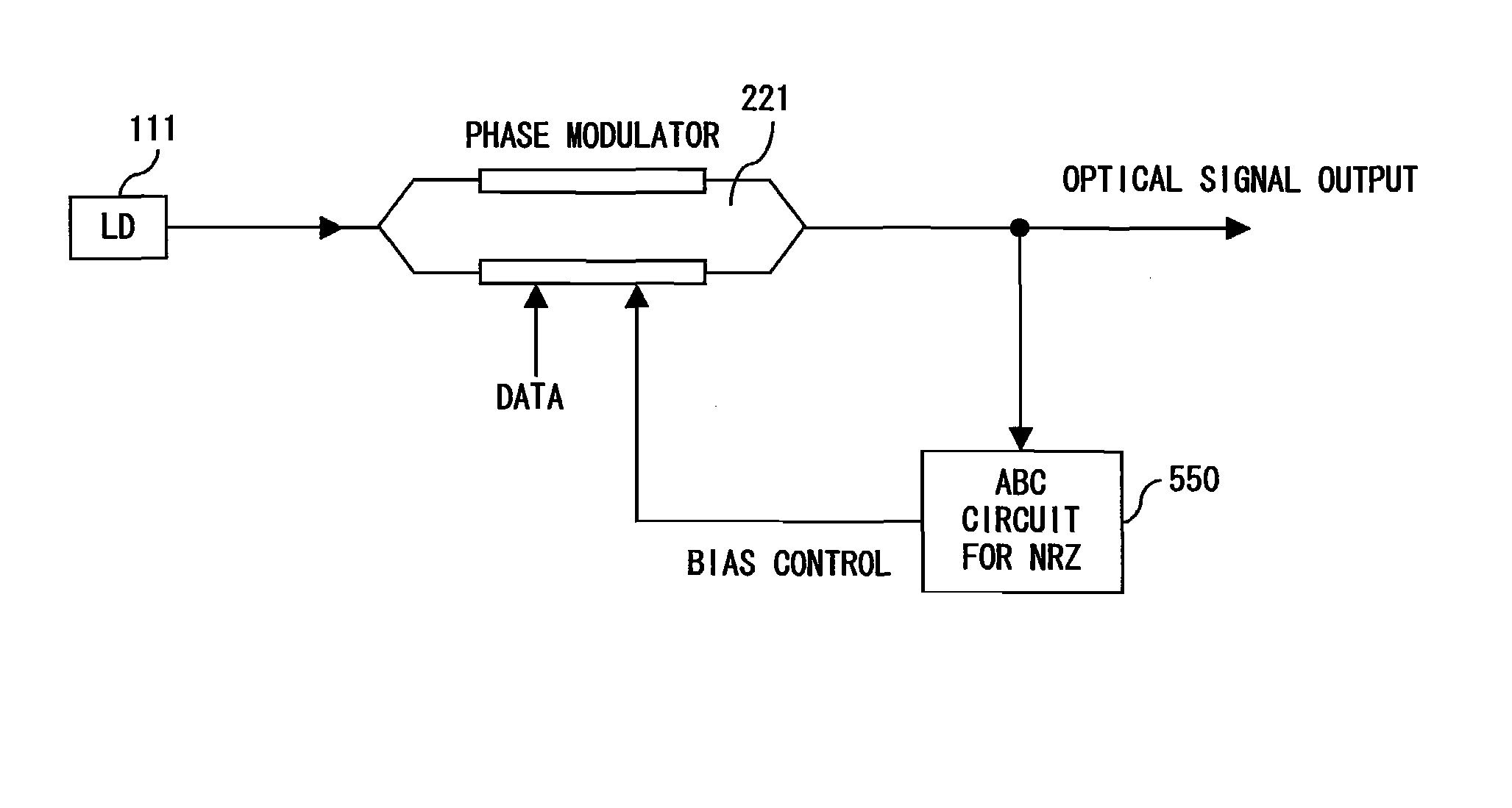
[0201] The first through the ninth embodiments has a configuration for controlling to maintain only the amount of phase shift of the phase shift unit at an appropriate value. The tenth embodiment, meanwhile, has a configuration to stabilize the operation of a whole optical transmitting apparatus.

[0202]FIG. 27 is a block diagram describing an entire configuration of the optical transmitting apparatus using DMPSK modulation (where M=2n). When “n=2”, it becomes DQPSK modulation, in which four values can be transmitted. FIG. 27 shows an entire configuration of the optical transmitting apparatus employing DQPSK modulation as an example of the DMPSK modulation. In FIG. 27, the illustration of the driving signal generator unit 110 and the clock signal generator unit 120 shown in FIG. 6 is omitted.

[0203] The optical transmitting apparatus shown in FIG. 27 comprises a clock signal generation unit; a driving signal generation unit for generating data signals DATA 1 and DATA 2 pre-coded for ...

eleventh embodiment

[0211] In the eleventh embodiment, like the tenth embodiment, a configuration for enhancing the stability of the operation of the entire optical transmitting apparatus. The eleventh embodiment, however, is an optical transmitting apparatus, which adopted a DBPSK modulation (i.e. n=1) among the DMPSK modulation (M=2n).

[0212]FIG. 30 is a block diagram of an optical transmitting apparatus using CSRZ (Carrier Suppressed Return-to-Zero)-DPSK modulation. An optical transmitting apparatus 105 shown in FIG. 30 comprises a driving signal generator 111 for generating a driving signal to be sent to a MZ modulator 113 using an input signal and a clock signal from a clock signal generator 112; a clock signal generator 112 for providing a clock signal to the driving signal generator 111 and a CSRZ intensity modulator 130; a CW optical source 115; a MZ modulator 113 comprising a plurality of modulating electrodes with input terminals for receiving data signals DATA 1 and DATA 2; the CSRZ intensit...

twelfth embodiment

[0232] In the DQPSK modulation, as explained referring to FIG. 3, each symbol comprises 2-bit data (DATA 1 and DATA 2). Either “0” or “π” is assigned to the data DATA 1, and either “π / 2” or “3π / 2” is assigned to the data DATA 2. Therefore, each of the symbols (00, 10, 11, 01) can be represented by “π / 4”, “3π / 4”, “5π / 4” and “7π / 4”.

[0233] In the twelfth embodiment, as shown in FIG. 38, “0” or “π+α” is assigned to the data DATA 1. “φ” or “φ+π+β” is assigned to the data DATA 2. Here, “φ” is the amount of phase shift by the phase shift unit, and is ideally “π / 2”. “α” and “β” are the phases added in the twelfth embodiment.

[0234] Signal points A and B corresponding to the data DATA 1, and signal points C and D corresponding to the data DATA 2 are represented as the following on the phase plane. A⁡(220)B⁡(-22⁢cos⁢ ⁢α-22⁢sin⁢ ⁢α)C⁡(22⁢cos⁢ ⁢ϕ22⁢sin⁢ ⁢ϕ)D⁡(-22⁢cos⁡(β+ϕ)-22⁢sin⁡(β+ϕ))

[0235] Signal points E, F, G and H corresponding to each of the symbols (00, 10, 11, 01) are represented as ...


PUM


Abstract

A phase shift unit provides a prescribed phase difference (π/2, for example) between a pair of optical signals transmitted via a pair of arms constituting a data modulation unit. A low-frequency signal f0 is superimposed on one of the optical signals. A signal of which phase is shifted by π/2 from the low-frequency signal f0 is superimposed on the other optical signal. A pair of the optical signals is coupled, and a part of which is converted into an electrical signal by a photodiode. 2f0 component contained in the electrical signal is extracted. Bias voltage provided to the phase shift unit is controlled by feedback control so that the 2f0 component becomes the minimum.

Description

CROSS-REFERENCE TO RELATED APPLICATION [0001] This is a continuation-in-part of application Ser. No. 11 / 256,128, filed on Oct. 24, 2005, which is now pending.BACKGROUND OF THE INVENTION [0002] 1. Field of the Invention [0003] The present invention relates to an optical transmitting apparatus, an optical receiving apparatus, and an optical communication system comprising them, and more specifically to an optical transmitting apparatus for transmitting an optical signal using PSK modulation, an optical receiving apparatus for receiving an optical signal from the optical transmitting apparatus, and an optical communication system comprising those apparatus. [0004] 2. Description of the Related Art [0005] Development of a practical implementation of an optical transmitting apparatus aiming to establish a high capacity and long distance optical transmission system has been awaited in recent years. Particularly, expectations for implementation of an optical transmitting apparatus, which e...

Claims


Application Information

Patent Timeline
IPC IPC(8): H04B10/04G02F1/03H04B10/516H04B10/07H04B10/548H04B10/61
CPCG02F1/0123G02F1/2255H04B10/505H04B10/5051H04B10/5053H04B10/50575H04B10/677H04B10/50595H04B10/5162H04B10/5165H04B10/5561H04B10/66H04B10/50577
Inventor AKIYAMA, YUICHIHOSHIDA, TAKESHIMIURA, AKIRAKAI, YUTAKAOOI, HIROKIRASMUSSEN, JENSNAKAMURA, KENTAROKUWATA, NAOKINISHIZAWA, YOSHINORITAKAHARA, TOMOOYUKI, MASAHIRO
Owner FUJITSU LTD
Why Eureka
Try Eureka