Storage system for wafers and other objects used in the production of semiconductor products
- Summary
- Abstract
- Description
- Claims
- Application Information
AI Technical Summary
Benefits of technology
Problems solved by technology
Method used
Image
Examples
Embodiment Construction
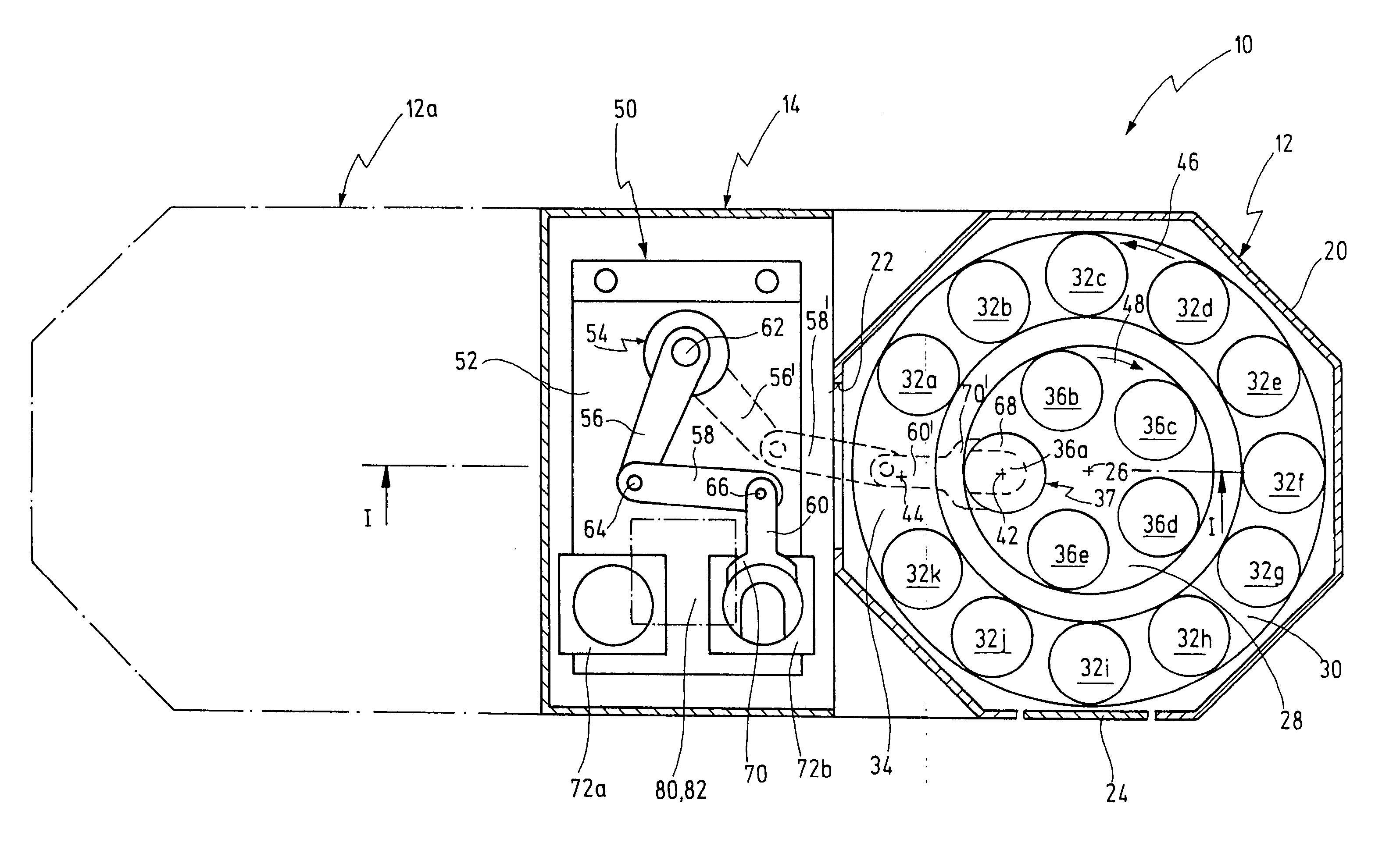
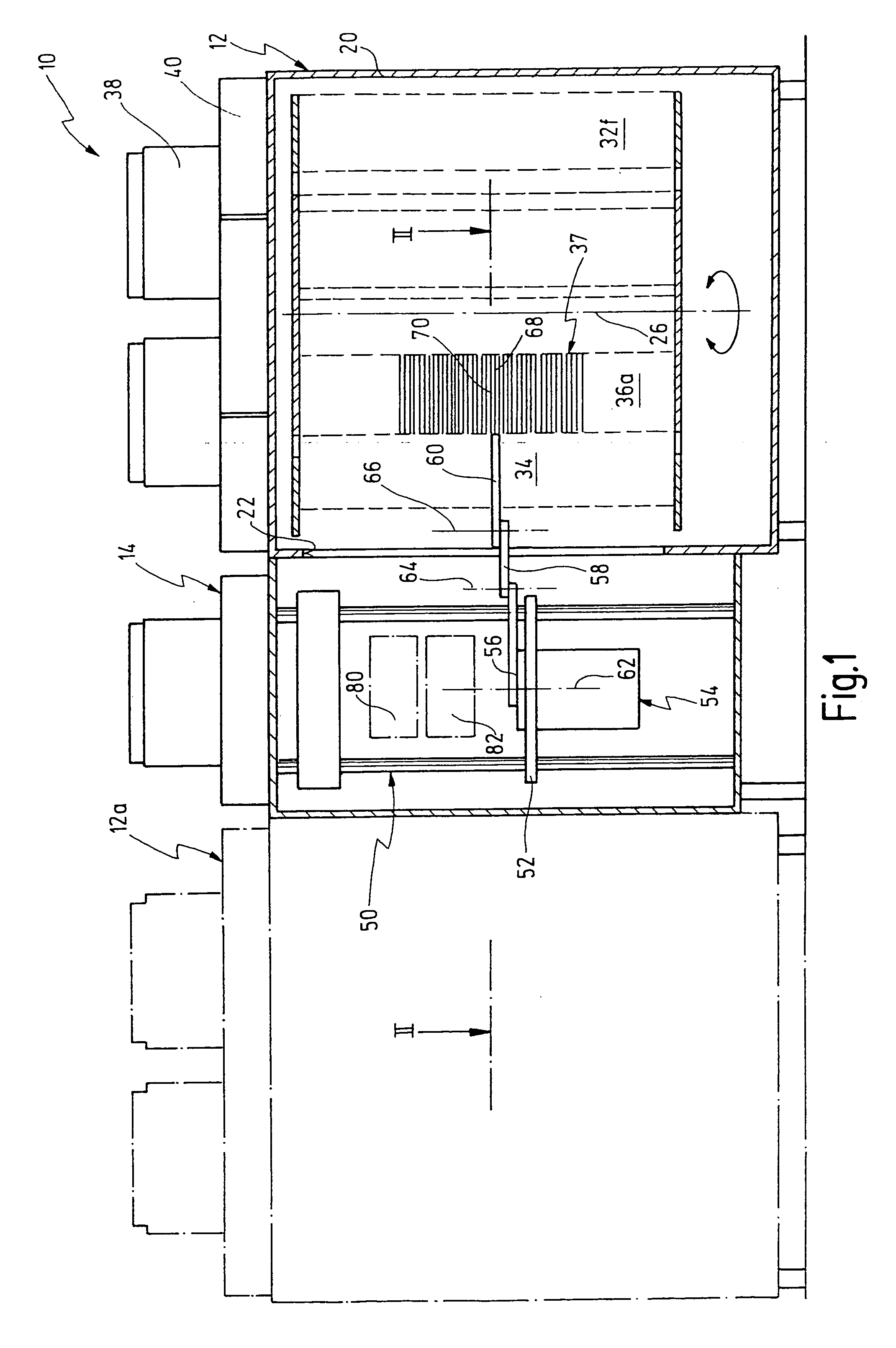
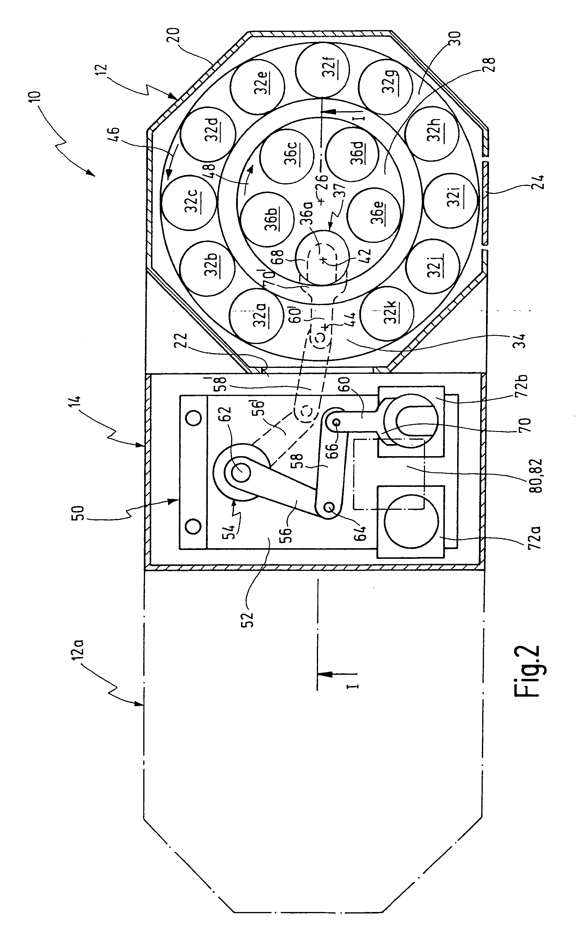
[0035] In FIGS. 1 and 2, a storage system for wafers is designated as a whole by 10. The concept of this storage system can also be applied to storage systems for reticles and other disk like objects used in the production of semiconductor products.
[0036] The storage system 10 has a storage module 12, which is laterally connected to an inserting and dispensing module 14. In exemplary embodiments of the invention there can even be two storage modules 12, 12a arranged on either side of the inserting and dispensing module 14, as indicated by dashed-dotted lines for a further storage module 12a. In addition, arrangements with three or more such storage modules are also conceivable.
[0037] The storage module 12 is provided with a closed housing 20, which merely has an opening 22 as an aperture at the transition to the inserting and dispensing module 14. Furthermore, a door 24 may be provided in the housing 20, in particular for servicing and repair purposes.
[0038] Inside the storage mo...
PUM
 Abstract
Description
Claims
Application Information


