Methods of forming devices associated with semiconductor constructions

Inactive Publication Date: 2006-11-23
ROUND ROCK RES LLC
View PDF7 Cites 24 Cited by
  • Summary
  • Abstract
  • Description
  • Claims
  • Application Information

AI Technical Summary

Problems solved by technology

Decreasing the size of transistor devices, however, leads to numerous difficulties.
For instance, as the channel-length of a transistor device is decreased, numerous problems occur in attempting to control electron flow between source / drain regions on opposing sides of the channel.
Although recessed access devices have advantages relative to non-recessed devices in terms of the packing density that can be achieved while avoiding short-channel effects, there are various problems encountered in large-scale fabrication of recessed access devices which are to be addressed if recessed access devices are to become commercially feasible.

Method used


Image

  • Methods of forming devices associated with semiconductor constructions
  • Methods of forming devices associated with semiconductor constructions
  • Methods of forming devices associated with semiconductor constructions

Examples


Embodiment Construction

[0029] This disclosure of the invention is submitted in furtherance of the constitutional purposes of the U.S. Patent Laws “to promote the progress of science and useful arts” (Article 1, Section 8).

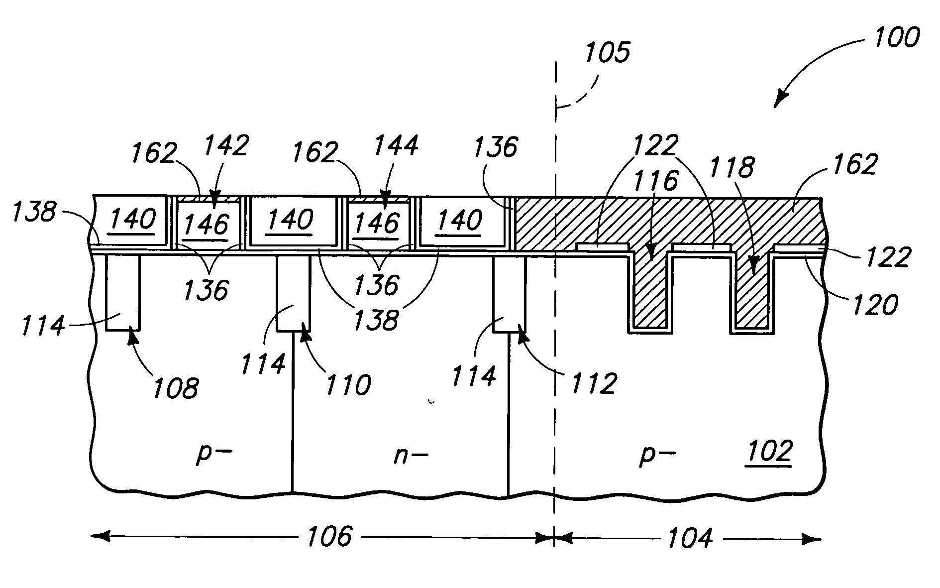
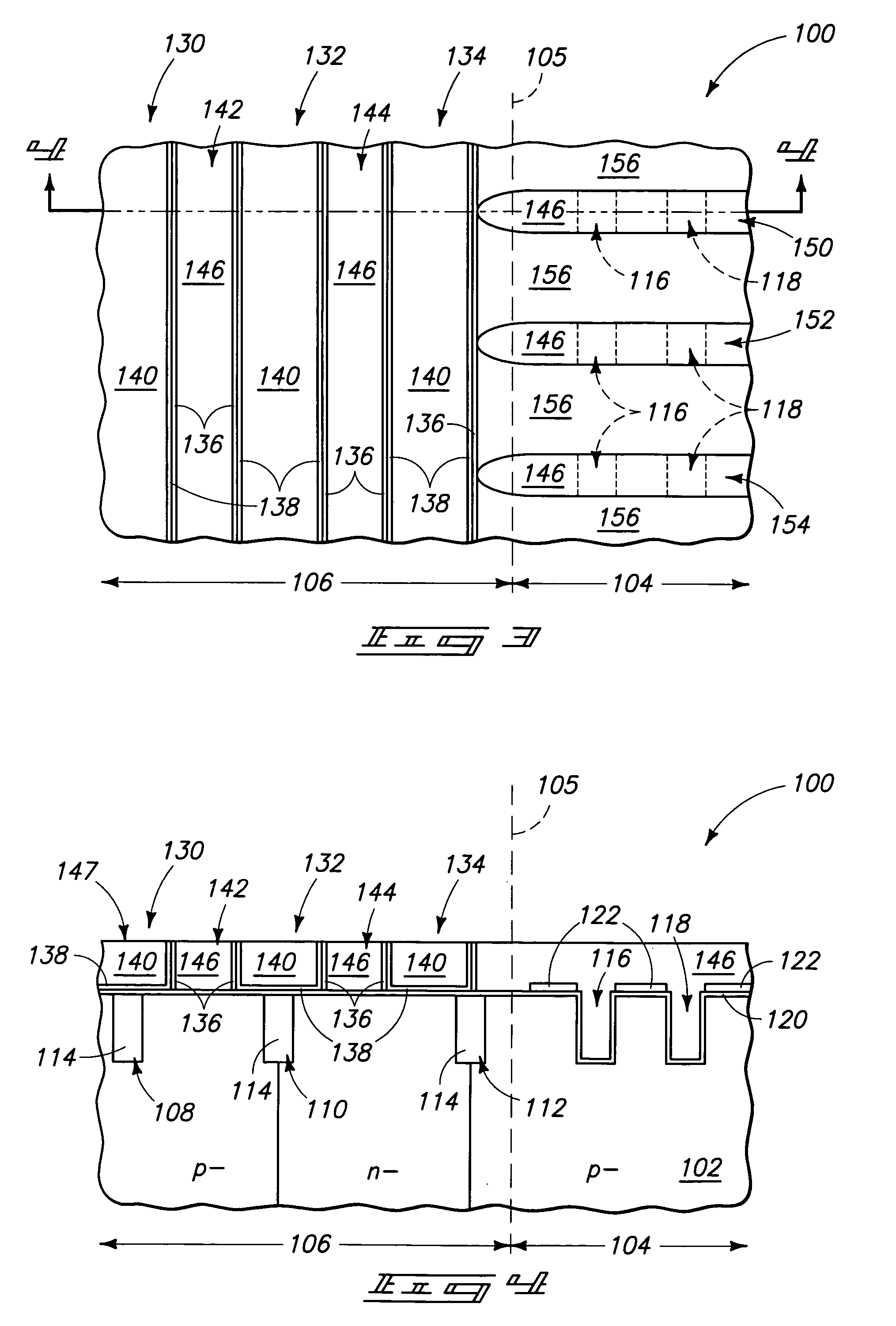
[0030] The invention includes processes for forming fully silicided metal gates in recessed access devices. The fully silicided metal gates can be utilized in, for example, 4.5 F2 cell designs. Semiconductor constructions will frequently have some fully silicided metal gates formed thereover, and some partially silicided gates. For instance, the fully silicided metal gates can be utilized in recessed access devices within a memory array, and the partially silicided gates can be utilized in transistor constructions peripheral to the memory array. The invention can include processing in which one or more steps utilized for formation of fully silicided recessed gates are conducted simultaneously with steps utilized to form partially silicided planar transistor gates.

[0031] Exemplary aspec...


PUM


Abstract

The invention includes methods of forming devices associated with semiconductor constructions. In exemplary methods, common processing steps are utilized to form fully silicided recessed array access gates and partially silicided periphery transistor gates.

Description

TECHNICAL FIELD [0001] The invention pertains to methods of forming devices associated with semiconductor constructions, and in particular aspects pertains to methods of forming recessed access devices (generally, metal-oxide-semiconductor field effect transistor, MOSFET, devices). BACKGROUND OF THE INVENTION [0002] A semiconductor transistor device is a device comprising a gate which interconnects a pair of source / drain regions with one another through a channel controlled by the gate. Transistor devices are common circuit devices of semiconductor constructions. For instance transistor devices can be incorporated into memory structures, including, for example, dynamic random access memory (DRAM) and static random access memory (SRAM). [0003] A continuing goal in semiconductor fabrication is to increase a level of integration, and thus decrease the amount of semiconductor real-estate consumed by devices. Decreasing the size of transistor devices, however, leads to numerous difficult...

Claims


Application Information

Patent Timeline
IPC IPC(8): H01L21/8242H01L21/22H01L21/4763H01L21/44H01L21/302H01L21/38
CPCH01L27/10876Y10S439/917H01L27/10897H01L27/10894H10B12/053H10B12/09H10B12/50
Inventor NEJAD, HASANHALLER, GORDON A.FIGURA, THOMAS ARTHURIYER, RAVI
Owner ROUND ROCK RES LLC
Why Eureka
Try Eureka