Electronic component and method for manufacturing the same

a technology of electronic components and manufacturing methods, applied in the field of electronic components, can solve the problems of electromagnetic mutual interference between active elements and structural defects in ceramic substrates, and achieve the effects of high reliability, preventing structural defects, and avoiding electromagnetic mutual interferen

Active Publication Date: 2006-11-30
MURATA MFG CO LTD
View PDF11 Cites 43 Cited by
  • Summary
  • Abstract
  • Description
  • Claims
  • Application Information

AI Technical Summary

Benefits of technology

[0009] To overcome the problems described above, preferred embodiments of the present invention provide a highly reliable electronic component in which electromagnetic mutual interference is prevented between an active element and a passive element and in which structural defects, such as delamination, are prevented, and also provide a method for manufacturing such an electronic component.

Problems solved by technology

However, the conventional electronic component, such as the high-frequency semiconductor device and the high-frequency module, is problematic in that electromagnetic mutual interference occurs between the active elements and the passive elements because the active elements and the passive elements are all disposed within the resin layer on one side of the ceramic substrate.
Even if such delamination is not produced, the significant change in volume may cause structural defects in the ceramic substrate, such as cracks and breakages.

Method used


Image

  • Electronic component and method for manufacturing the same
  • Electronic component and method for manufacturing the same
  • Electronic component and method for manufacturing the same

Examples


Embodiment Construction

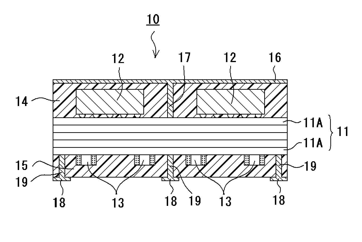
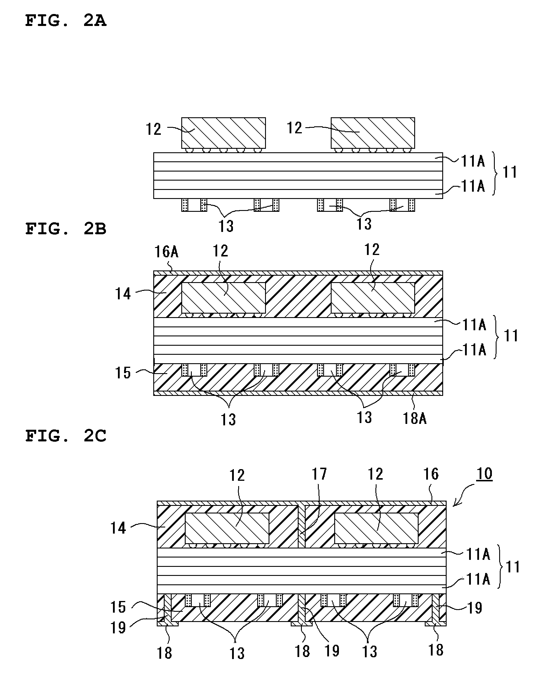
[0020] The present invention will now be described first with reference to a preferred embodiment shown in FIG. 1. FIG. 1 is a cross-sectional view of an electronic component according to a preferred embodiment of the present invention. FIGS. 2A-2C illustrate a relevant portion in a method for manufacturing the electronic component according to a preferred embodiment of the present invention, FIG. 2A is a cross-sectional view showing a state where active elements and passive elements are set on a core substrate, FIG. 2B is a cross-sectional view showing a state where resin layers are pressure-bonded to the core substrate shown in FIG. 2A, and FIG. 2C is a cross-sectional view showing a finished product of the electronic component provided with via-hole conductors.

[0021] For example, referring to FIG. 1, an electronic component 10 according to the present preferred embodiment includes a core substrate 11 including a multilayer resin substrate having a plurality of resin layers 11A, ...


PUM


Abstract

In an electronic component, an active chip element and a passive chip element are respectively enclosed within first and second resin layers, which are separately disposed on upper and lower surfaces of a core substrate, respectively. The first resin layer includes a shielding metal film disposed on an upper surface thereof and a first via-hole conductor which connects the shielding metal film with a circuit pattern provided on the core substrate. The second resin layer includes an external-terminal electrode disposed on a lower surface thereof and a second via-hole conductor which connects the external-terminal electrode with a circuit pattern provided on the core substrate.

Description

BACKGROUND OF THE INVENTION [0001] 1. Field of the Invention [0002] The present invention relates to an electronic component having an active element and a passive element that are resin-sealed to a substrate, and to a method for manufacturing the same. In particular, the present invention relates to an electronic component that is highly reliable both electrically and structurally, and to a method for manufacturing the same. [0003] 2. Description of the Related Art [0004] As a conventional electronic component of this type, a high-frequency semiconductor device disclosed in Japanese Unexamined Patent Application Publication No. 2003-124435 (Patent Document 1), and a high-frequency module and method for manufacturing the high-frequency module disclosed in Japanese Unexamined Patent Application Publication No. 2002-033419 (Patent Document 2) are known. [0005] In the high-frequency semiconductor device according to Patent Document 1, a composite resin material layer composed of epoxy ...

Claims


Application Information

Patent Timeline
Patent Type & Authority Applications(United States)
IPC IPC(8): H01L23/552H01L23/00H01L23/31H01L25/04H01L25/065H01L25/18
CPCH01L23/3121H01L23/552H01L25/0655H01L2224/16H01L2224/16225H01L2924/01078H01L2924/19041H01L2924/19106H01L2924/3025H01L2924/01004H01L2924/00014H01L2924/00011H01L2224/0401H01L25/04H01L25/18H01L23/00
Inventor YAMAMOTO, YUKIHARADA, JUNTAKAGI, HIROSHIHIRAYAMA, KATSURO
Owner MURATA MFG CO LTD
Why Eureka
Try Eureka