Optical image stabilizer for camera lens assembly

Inactive Publication Date: 2006-11-30
SAMSUNG ELECTRONICS CO LTD
View PDF6 Cites 16 Cited by
  • Summary
  • Abstract
  • Description
  • Claims
  • Application Information

AI Technical Summary

Benefits of technology

[0017] It is, therefore, an object of the present invention to provide an optical image stabilizer for a camera lens assembly, which can be embedded in a small-size and lightweight photographing devic

Problems solved by technology

As the mobility of a camera lens assembly mounted in a mobile communication terminal increases, image blurring caused by fine vibration or handshaking represents a serious impediment to high quality images.
Although high-definition cameras have emerged with the development of optical technology, they lose half their effect due to image blurring caused by vibration, thus, increasing a need for an image stabilizer.
However, adjustment using a program requires a separate memory or a high-performance camera device.
Moreover, a photographing speed may decrease as time required for correcting of a blurred image increases.
In addition, the extent to which an afterimage is removed using a program is limited, resulting in degradation of correction.
In the case of the optical image stabilizer, installation of a separate correction device increases a manufacturing cost and requires an installation space.
But there is a limit in using the correction technique for a small-size digital camera or mobile communication terminal having space constraints.
As a result, the handshaking correction device is difficult to mount on a mobile communication terminal where the length and outer diameter of a camera lens assembly are

Method used


Image

  • Optical image stabilizer for camera lens assembly
  • Optical image stabilizer for camera lens assembly
  • Optical image stabilizer for camera lens assembly

Examples


first embodiment

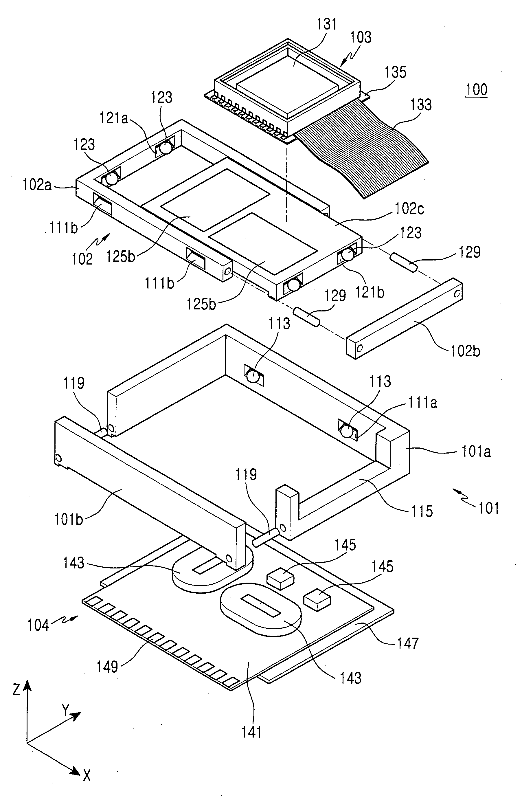
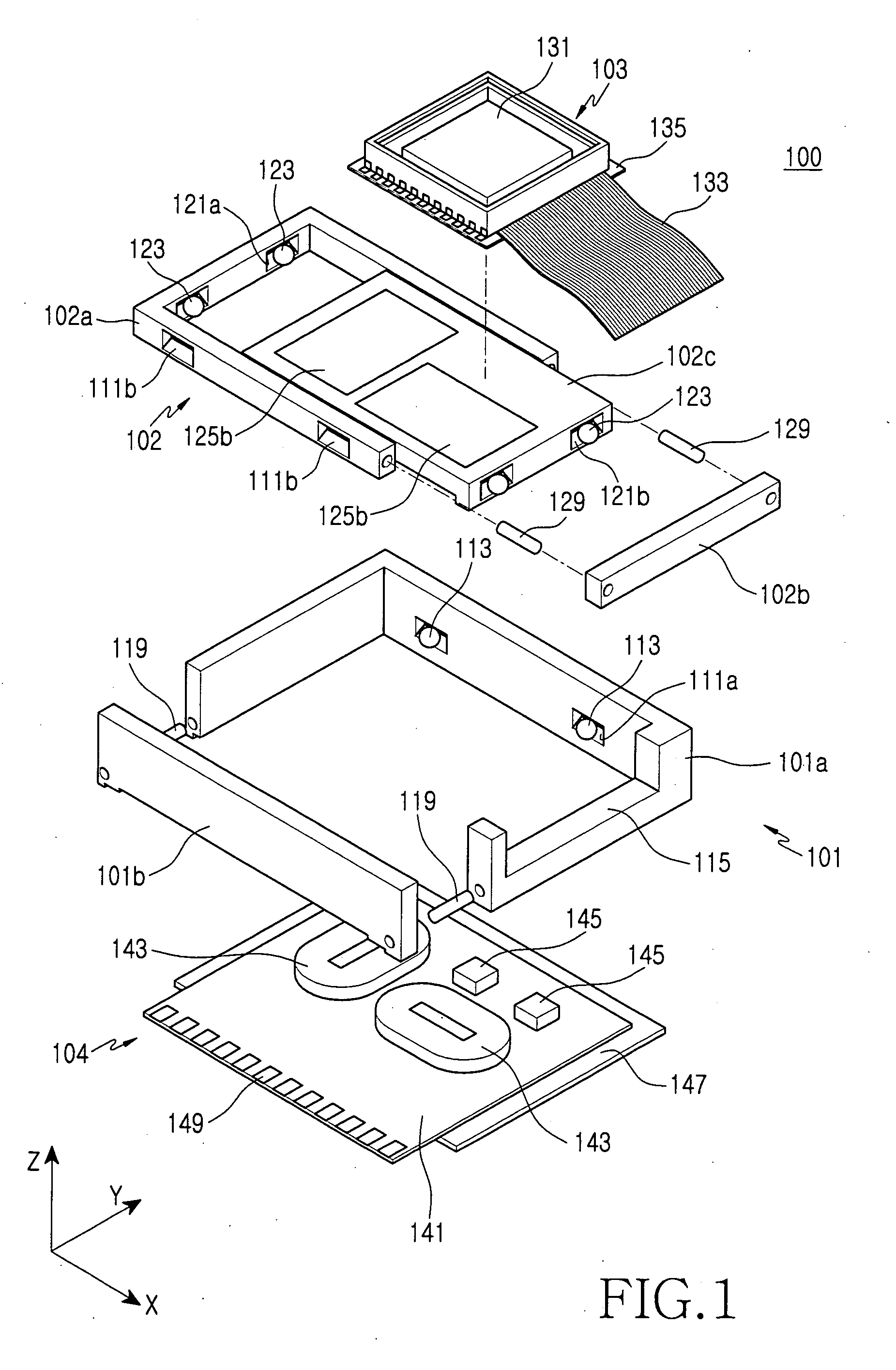
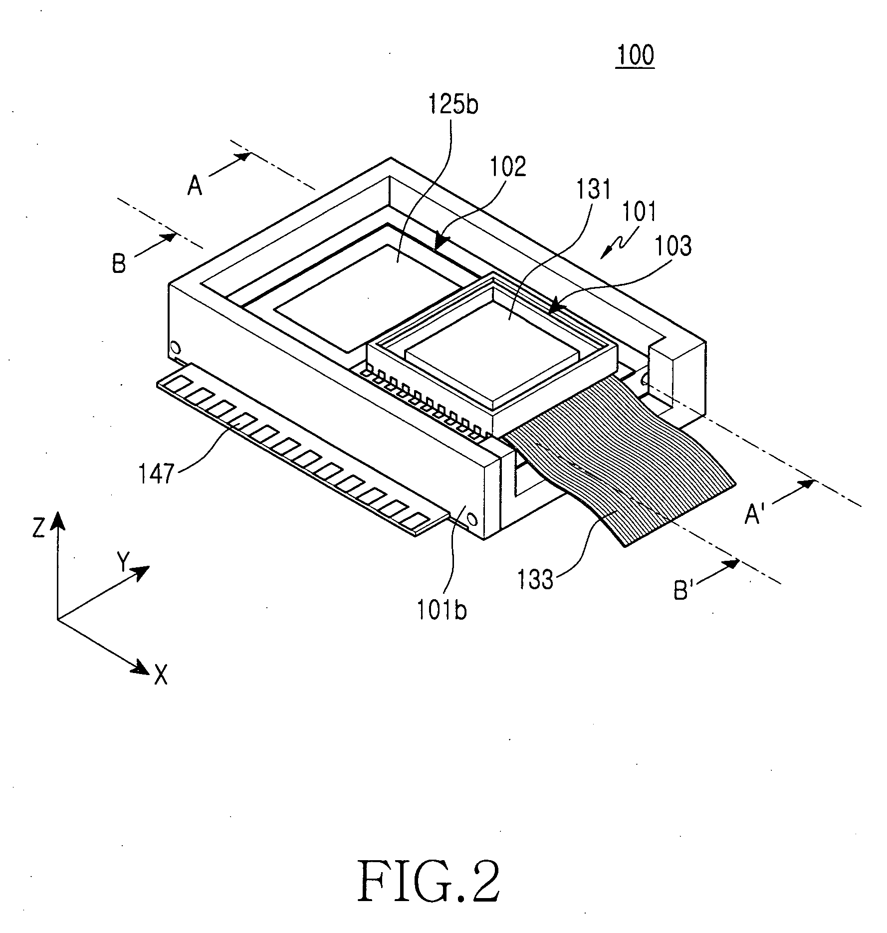
[0034] As shown in FIGS. 1 through 3, an optical image stabilizer 100 for a camera lens assembly according to the present invention, FIG. 1 illustrates an exploded perspective view of optical image stabilizer 100. FIG. 2 illustrates an assembled view of optical image stabilizer 100 and FIG. 3 illustrates cross-sectional views of optical image stabilizer 100 along Sections A-A′ and B-B′, respectively. Referring to FIG. 1, optical image stabilizer 100 includes a main frame 101, a driving frame 102, a coil 143, and a permanent magnet (125a of FIG. 3), in which the driving frame 102 moves on the main frame 101 through interaction between the coil 143 and the permanent magnet 125a to change the position of a camera device 103, thereby correcting for blurring of a captured image due to user's handshaking.

[0035] At least a portion of the top of the main frame 101 is opened to allow a subject image to incident to the camera device 103. At least one first sliding groove 111a is formed in inn...

second embodiment

[0060] In the optical image stabilizer 200 according to the present invention, a coil portion 204, more specifically a printed circuit board (PCB) 241 of the coil portion 204 is mounted on the second frame 202c.

[0061] The coils 243 and the position detecting sensors 245 are mounted on the bottom surface of the PCB 241. Once the PCB 241 is assembled onto the second frame 202c, the coils 243 and the position detecting sensors 245 are surrounded by the second frame 202c. A circuit pattern (not shown) capable of transmitting a signal generated by the position detecting sensors 245 while applying a voltage to the coils 243 and the position detecting sensors 245 is mounted on the PCB 241. The PCB 241 is supplied with a voltage through the circuit pattern and a predetermined connector 249 or transmits a signal generated by the position detecting sensors 245. The camera device 103 mounted on the PCB 241 is positioned on the second frame 202c.

[0062] The bottom of the main frame 201 is clos...

third embodiment

[0063]FIGS. 7 through 9 illustrate an optical image stabilizer 300 for a camera lens assembly according to the present invention. FIG. 7 illustrates an exploded perspective view of optical image stabilizer 300. FIG. 8 illustrates an assembled view of optical image stabilizer 300 and FIG. 9 illustrates a cross-sectional view of optical image stabilizer 300 along Sections C-C′. Referring to FIG. 7, optical image stabilizer 300 is similar to the embodiments of the invention shown in FIGS. 1 and 4 but has a reduced thickness from the preceding embodiments of the present invention as camera device 303 is mounted at a side of and positioned in the same plane as second frame 302c.

[0064] The optical image stabilizer 300 includes a main frame 301, a driving frame 302, and the camera device 303 mounted at a side of the second frame 302c of the driving frame 302.

[0065] The main frame 301 includes a first frame member 301a whose side along the second direction, Y, is opened and a second frame...


PUM


Abstract

Disclosed is an optical image stabilizer assembly for a camera lens. The optical image stabilizer includes a main frame, a driving frame, a camera device, a pair of driving permanent magnets, a pair of coils, and at least one slidable bearing between the main frame and the driving frame. The driving frame moves in at least one direction within the main frame. The camera device is mounted on the driving frame. The pair of driving permanent magnets is mounted on one of the main frame and the driving frame. The pair of coils is mounted on the other of the main frame and the driving frame and faces the pair of driving permanent magnets. The one slidable bearing is interposed between an inner sidewall of the main frame and an outer sidewall of the driving frame to facilitate movement of the driving frame. The driving frame moves through interaction between an electromagnetic force generated by application of a current to the coils and a magnetic force of the driving permanent magnets.

Description

CLAIM OF PRIORITY [0001] This application claims the benefit, pursuant to 35 U.S.C. § 119, to that patent application entitled “Optical Image Stabilizer for Camera Lens Assembly,” filed in the Korean Intellectual Property Office on May 31, 2005 and assigned Serial No. 2005-46337, the contents of which are incorporated herein by reference. BACKGROUND OF THE INVENTION [0002] 1. Field of the Invention [0003] The present invention generally relates to a camera lens assembly, and in particular, to an optical image stabilizer for stabilizing an image blurred by movement when a digital camera or an optical device mounted in a mobile communication terminal photographs a subject. [0004] 2. Description of the Related Art [0005] With the miniaturization of digital cameras and development of lightweight techniques, mobile communication terminals or devices having optical lenses and camera devices have come into wide use. [0006] As the mobility of a camera lens assembly mounted in a mobile commu...

Claims


Application Information

Patent Timeline
IPC IPC(8): G03B17/00
CPCG02B27/646G03B5/02H04N5/23287H04N5/23248H04N5/23258H04N5/2253H04N23/54H04N23/68H04N23/6812H04N23/687
Inventor KIM, HEE-SEUNGLEE, JONG-PILSHIN, DOO-SIKSHIN, JEONG-KIL
Owner SAMSUNG ELECTRONICS CO LTD
Why Eureka
Try Eureka