

Substrate structure and manufacturing method of the same
a technology of substrate structure and manufacturing method, which is applied in the direction of material nanotechnology, semiconductor devices, semiconductor/solid-state device details, etc., can solve the problems of damage to other portions of the substrate, and it is extremely difficult to form a microstructure represented by various kinds of wirings using the cnts, and achieve the effect of linear structur
- Summary
- Abstract
- Description
- Claims
- Application Information
AI Technical Summary
Benefits of technology
Problems solved by technology
Method used
Image

Examples
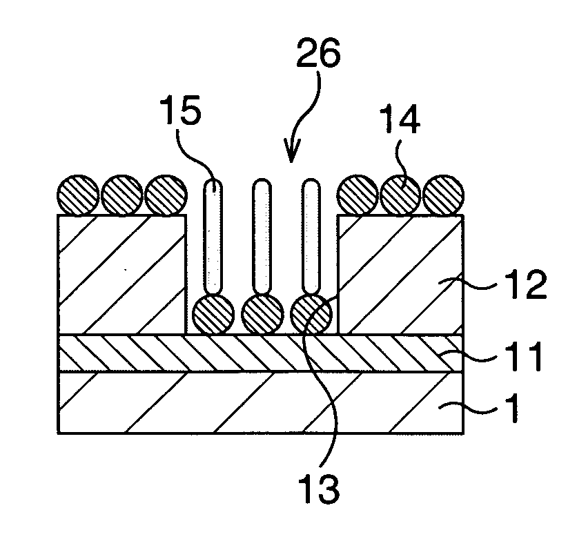
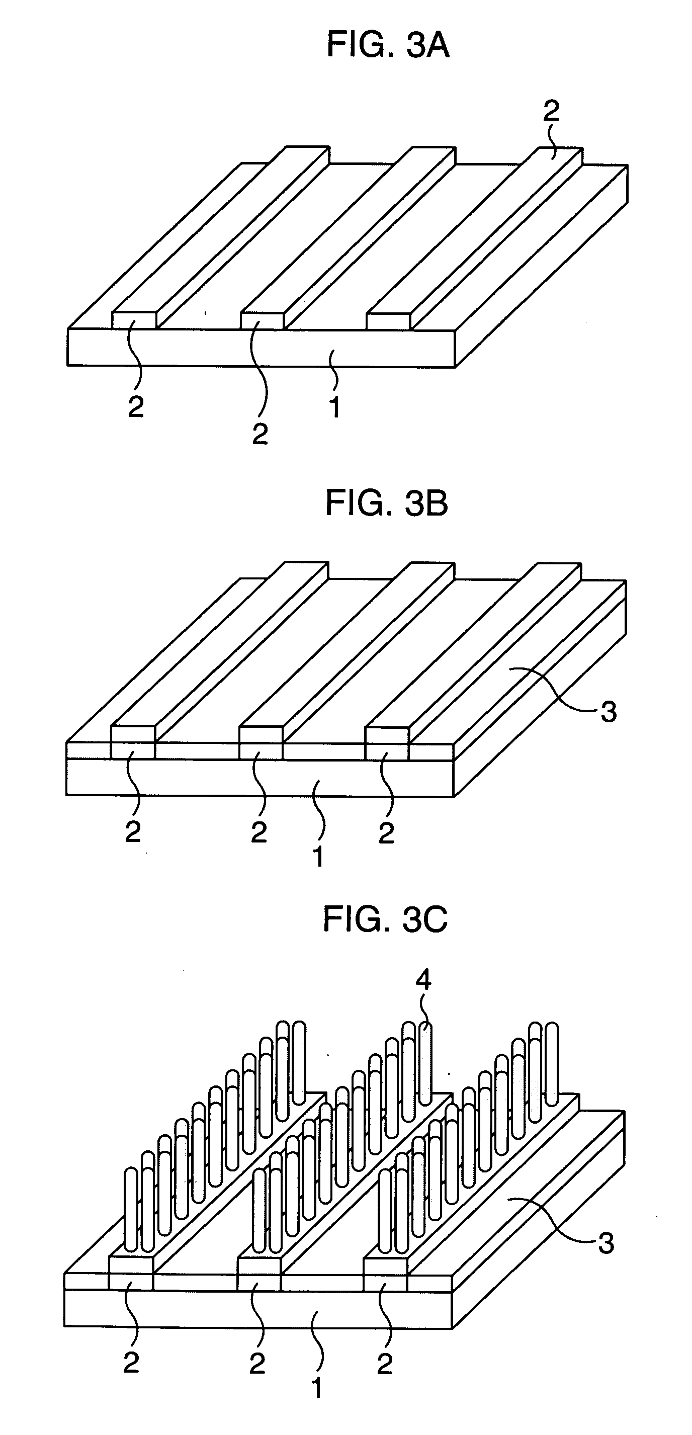
first embodiment
[0057]FIG. 3A to FIG. 3C are schematic perspective views showing main steps of a manufacturing method of a substrate structure according to the first embodiment.
[0058] In this embodiment, first, as shown in FIG. 3A, a Ti film 2 as a base film is deposited, for example, to have a thickness of approximately 1 nm on a silicon substrate 1, for example, by a sputtering method. This Ti film 2 is fabricated in a desired shape, in the example shown, in a band shape by photolithography and dry etching.
[0059] Subsequently, as shown in FIG. 3B, a catalyst material, here, a Co film 3 is formed to have a thickness of approximately 1 nm on the entire surface of the silicon substrate 1 so as to cover the band-shaped Ti film 2, for example, by the sputtering method.
[0060] Thereafter, the Co film 3 is subjected to CNT growth processing by the CVD method.
[0061] More specifically, by the thermal CVD method, the growth processing is executed with the growth temperature (environmental temperature in...
second embodiment
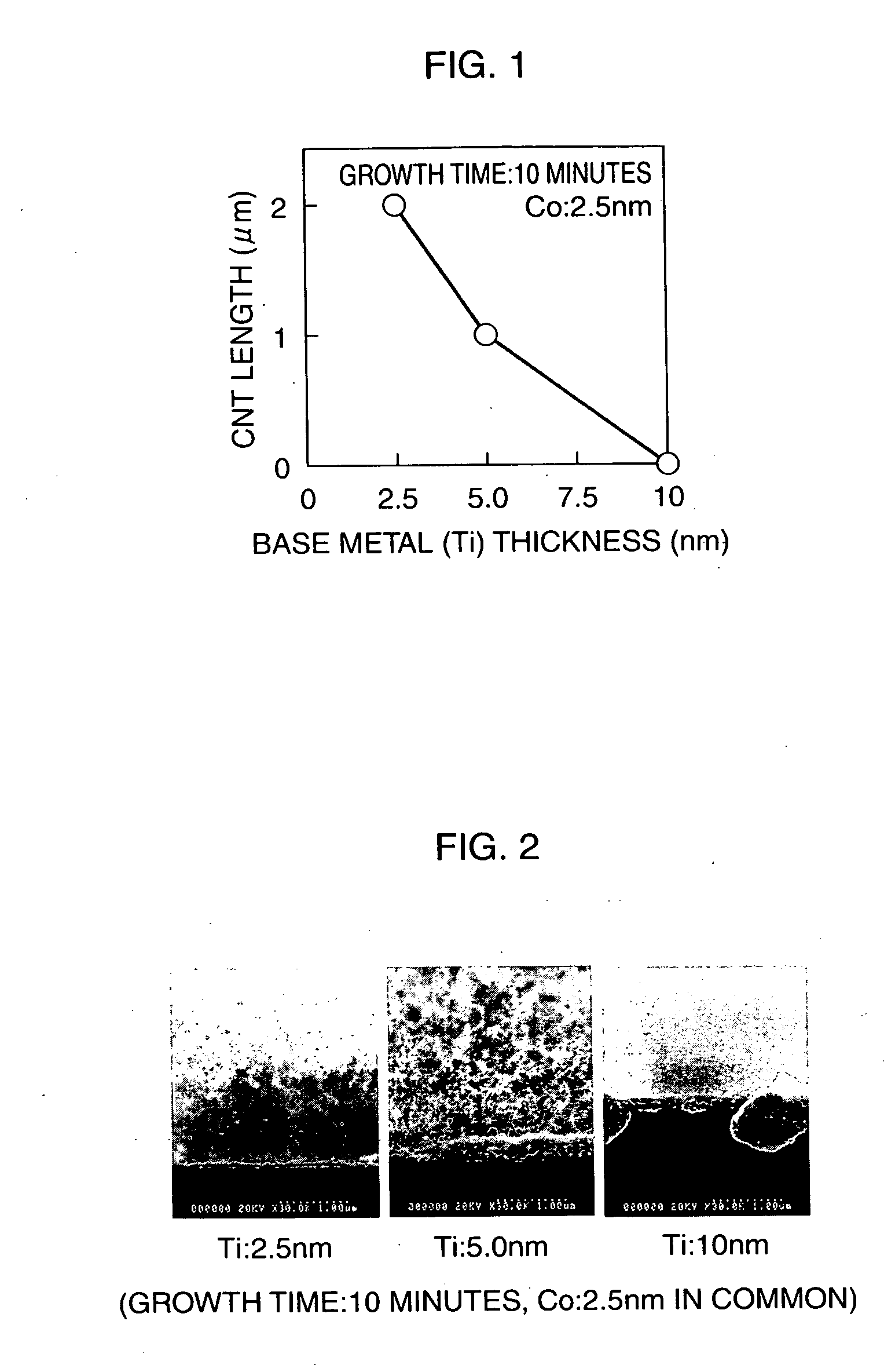
[0094] In this embodiment, specific examples in which a portion where CNTs are formed is controlled using a base film as in the first embodiment are disclosed, but this embodiment is different in that the portion where the CNTs are formed and the lengths of the CNTs are controlled by adjusting the thickness of the base film.
[0095]FIG. 9A to FIG. 9C are schematic perspective views showing main steps of a manufacturing method of a substrate structure according to the second embodiment.
[0096] In this embodiment, first, as shown in FIG. 9A, a Ti film 41 as a base film is deposited, for example, to have a thickness of approximately 1 nm on the silicon substrate 1, for example, by the sputtering method. Then, this Ti film 41 is fabricated in a desired shape, in the example shown, in a band shape by photolithography and dry etching.
[0097] Subsequently, a photoresist (not shown) is applied thicker than the Ti film 41 onto the entire surface of the silicon substrate 1, and a desired shape...
third embodiment
[0132]FIG. 13A and FIG. 13B are schematic perspective views showing main steps of a manufacturing method of a substrate structure according to the third embodiment.
[0133] In the beginning, as shown in FIG. 13A, a band-shaped Ti film 102 is formed, and Co particles 103 are scattered over the entire surface.
[0134] First, the Ti film 102 as a base film is deposited, for example, to have a thickness of approximately 1 nm on a silicon substrate 101, for example, by the sputtering method. This Ti film 102 is fabricated in a desired shape, in the example shown, in a band shape by photolithography and dry etching.
[0135] Incidentally, after an insulating film such as a silicon oxide film is formed on the entire surface of the silicon substrate 101, the Ti film 102 and so on may be formed on this insulating film.
[0136] Then, plural catalyst particles, here the Co particles 103 are formed on the entire surface of the silicon substrate 101 including a portion on the band-shaped Ti film 102 ...
PUM
| Property | Measurement | Unit |
|---|---|---|
| thickness | aaaaa | aaaaa |
| thickness | aaaaa | aaaaa |
| thickness | aaaaa | aaaaa |
Abstract
Description
Claims
Application Information