Dead time control circuit capable of adjusting temperature characteristics of dead time

a control circuit and dead time technology, applied in logic circuit coupling/interface arrangement, pulse technique, instruments, etc., can solve the problems of dead time, inability to adjust delay time, above-described second prior art dead time control circuit, increase in size and manufacturing cost,

a control circuit and dead time technology, applied in logic circuit coupling/interface arrangement, pulse technique, instruments, etc., can solve the problems of dead time, inability to adjust delay time, above-described second prior art dead time control circuit, increase in size and manufacturing cost,

US20060290401A1Active Publication Date: 2006-12-28RENESAS ELECTRONICS CORP

Image

  • Dead time control circuit capable of adjusting temperature characteristics of dead time
  • Dead time control circuit capable of adjusting temperature characteristics of dead time
  • Dead time control circuit capable of adjusting temperature characteristics of dead time

Examples


Embodiment Construction

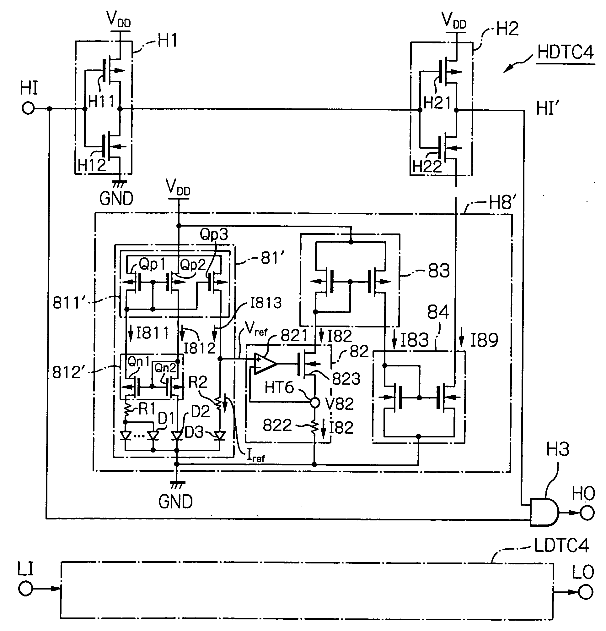
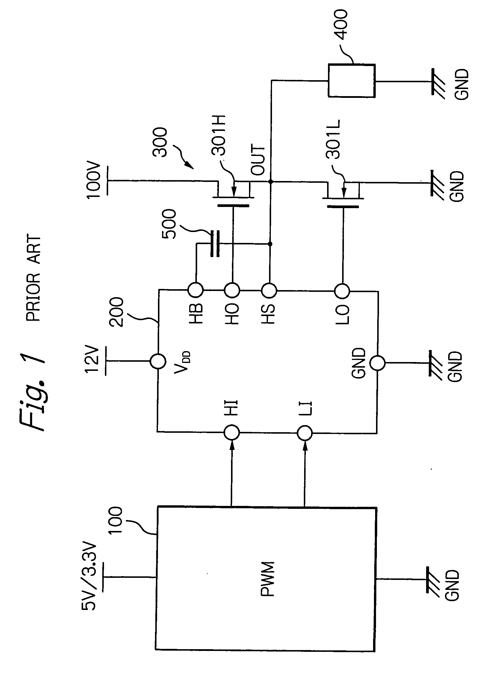
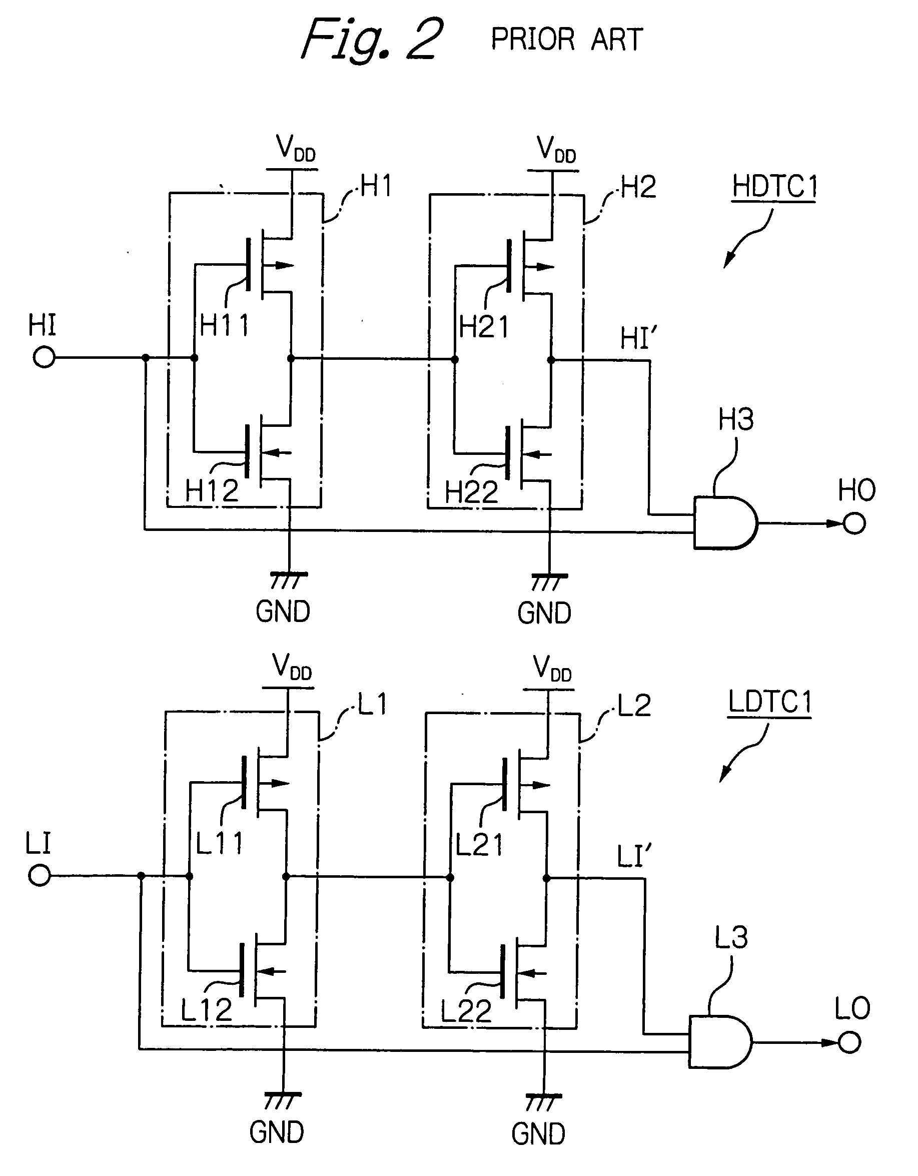
[0027] Before the description of the preferred embodiments, prior art dead time control circuits will be explained with reference to FIGS. 1, 2, 3, 4, 5 and 6.

[0028] In FIG. 1, which illustrates a prior art digital audio apparatus, a pulse width modulator 100 powered by a relatively low power supply voltage such as 5V or 3V generates output voltages and transmits them to a high-side input terminal HI and a low-side input terminal LI of a predriver 200 powered by a relatively high power supply voltage such as 12V at its power supply terminal VDD. The predriver 200 generates output voltages at their high-side output terminal HO and low-side output terminal LO and transmits them to a half bridge circuit or a push-pull type output buffer 300 powered by a commercial power supply voltage such as 100V.

[0029] The push-pull type output buffer 300 receives the output voltages at the high-side output terminal HO and the low-side output terminal LO of the predriver 200 to generate an output v...


PUM


Abstract

In a dead time control circuit, a delay circuit is connected to an input terminal and adapted to delay signals therethrough by a delay time corresponding to a dead time. A logic circuit has a first input connected via the delay circuit to the input terminal, a second input connected directly to the input terminal, and an output connected to an output terminal. The dead time having adjustable temperature characteristics.

Description

BACKGROUND OF THE INVENTION [0001] 1. Field of the Invention [0002] The present invention relates to a dead time control circuit used in a predriver for driving a half bridge circuit or a push-pull type output buffer for driving a load. [0003] 2. Description of the Related Art [0004] In a push-pull type output buffer, two switching elements are connected between a power supply terminal and a ground terminal. When the switching elements are alternately turned ON and OFF to drive a load connected thereto, if the switching elements are simultaneously turned ON, a large penetration current flows through the push-pull type output buffer, so that the switching elements would be broken down. [0005] In order to avoid such a large penetration current, a simultaneous-OFF time or a dead time is introduced between the ON times of the switching elements. Generally, two dead time control circuits each corresponding to one of the switching elements are provided. [0006] A first prior art dead time ...

Claims


Application Information

Patent Timeline
28 Dec 2006
Publication
US20060290401A1
IPC
H03H11/26; H03K5/13; H03K17/14; H03K17/284
CPC
H02M1/38; H02M2001/385; H03H11/265; H03K2005/00202; H03K5/1515; H03K2005/00143; H03H11/54; H02M1/385
Inventors
YANAGIGAWA, HIROSHI; YOSHIDA, MITSURU