Organic light-emitting device and organic light-emitting display

a light-emitting display and organic technology, applied in static indicating devices, instruments, electroluminescent light sources, etc., can solve the problems of inability to put into practical use, insufficient current charge of storage capacitors (csts), etc., and achieve the effect of improving the ability to display low gray levels

Active Publication Date: 2006-12-28
LG DISPLAY CO LTD
View PDF8 Cites 33 Cited by
  • Summary
  • Abstract
  • Description
  • Claims
  • Application Information

AI Technical Summary

Benefits of technology

[0018] An advantage of the present invention is to solve at least the problems and disadvantages of the background art.
[0019] Another advantage of the present invention is to provide an organic light-emitting device and an organic light-emitting display using the same, in which when a low gray level is displayed, a storage capacitor is sufficiently charged, thereby improving a capability to display low gray levels.
[0020] Additional features and advantages of the invention will be set forth in the description which follows, and in part will be apparent from the description, or may be learned by practice of the invention. The objectives and other advantages of the invention will be realized and attained by the structure particularly pointed out in the written description and claims hereof as well as the appended drawings.
[0021] To achieve these and other advantages and in accordance with the purpose of the present invention, as embodied and broadly described, an organic light-emitting device including: a light emitting diode that emits light by a signal current; a driving thin film transistor connected between a source voltage and a light emitting diode and connected at its drain to the light emitting diode and a current source, and that supplies the signal current to the light emitting diode depending on display data; a storage capacitor connected between the source voltage and a gate of the driving thin film transistor, and that stores the display data depending on a display data signal; a first switching unit connected between the drain of the driving thin film transistor and a data driver and connected at its gate with a first scan line, wherein the first switching unit and selects the data signal; a second switching unit connected between the gate and the drain of the driving thin film transistor and connected at its gate with a second scan line wherein, the second switching unit drives the driving thin film transistor; and a third switching unit connected between the drain of the driving thin film transistor and the light emitting diode and connected at its gate with a third scan line, wherein the third switch unit selects the signal current applied to the light emitting diode.
[0022] In another aspect of the present invention, an organic light-emitting device including: a storage capacitor that stores a da

Problems solved by technology

However, the conventional organic light-emitting device has a drawback in that when a low gray level is displayed, in comparison a current supplied from a data driver is dozens of nA.
In other words, the conventional organic light-emitting device has a drawback in that when a low gray level is displayed, due to the data line load, the storage capacitor (Cst

Method used


Image

  • Organic light-emitting device and organic light-emitting display
  • Organic light-emitting device and organic light-emitting display
  • Organic light-emitting device and organic light-emitting display

Examples


first embodiment

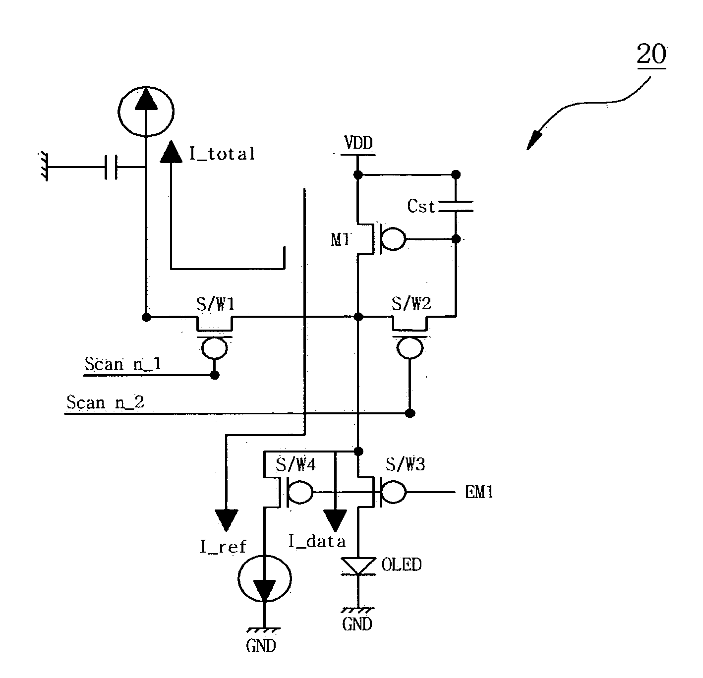
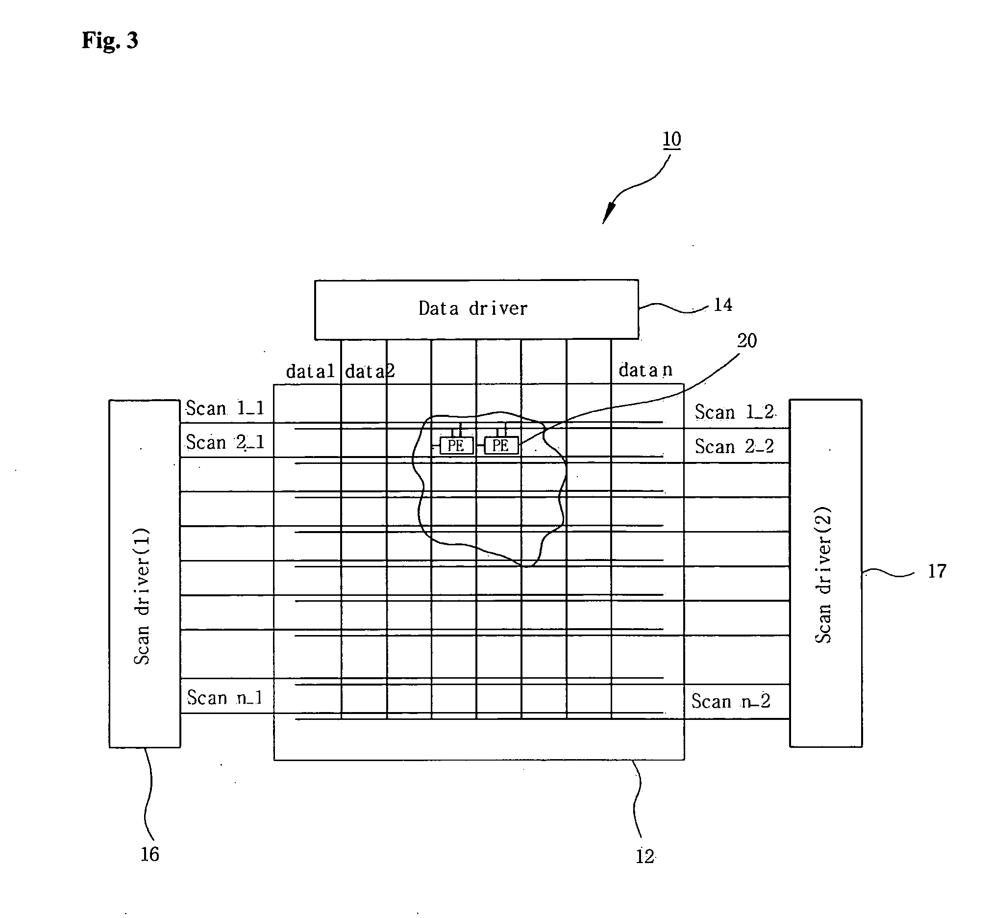
[0039]FIG. 3 illustrates the structure of an organic light-emitting display according to the first embodiment of the present invention.

[0040] Referring to FIG. 3, the organic light-emitting display 10 includes a pixel circuit 12, a data driver 14, and two scan drivers 16 and 17. The pixel circuit 12 receives data signals (data 1, data 2, . . . , data n) from the data driver 14 through a plurality of data lines, and receives scan signals (scan 1_1, scan 2_1 . . . scan n_1 / scan 1_2, scan 2_2 . . . scan n_2) from the scan drivers 16 and 17 through a plurality of scan lines. The pixel circuit 12 has a plurality of organic light-emitting devices 20 disposed at intersections of the data lines and the scan lines and emits light according to the data signal and the scan signal.

[0041]FIG. 4 illustrates the structure of the data driver and the pixel circuit of FIG. 3. The data driver 14 and the pixel circuit part 12 will be described in detail with reference to FIG. 4.

[0042] Referring to F...

second embodiment

[0058]FIG. 7 is an equivalent circuit diagram illustrating an organic light-emitting device according to the second embodiment of the present invention, and FIG. 8 is a plot showing current versus driving timing for FIG. 7.

[0059] Referring to FIGS. 7 and 8, the organic light-emitting device 30 is a current driving active matrix organic light-emitting device and is the same as the organic light-emitting device 20 according to the first embodiment of the present invention regarding its connections to the driving TFT (M1), first to third switches (S / W1 to S / W3), the storage capacitor (Cst), and the organic light-emitting diode (OLED).

[0060] However, the inventive organic light-emitting device 30 excludes a fourth switch (S / W4) unlike the organic light-emitting device 20 according to the second embodiment. If the first and second scan signals (scan n_1 and scan n_2) are applied to the gates of the first and second switches (S / W1 and S / W2), respectively, the driving TFT (M1) is turned ...

third embodiment

[0064]FIG. 9 is an equivalent circuit diagram illustrating an organic light-emitting device according to the third embodiment of the present invention. A plot showing current versus timing of the organic light-emitting device according to the third embodiment of the present invention is the same as that of FIG. 6. Accordingly, FIG. 6 is referred to.

[0065] Referring to FIGS. 6 and 9, the inventive organic light-emitting device 40 is a current driving active matrix organic light emitting device and is the same as the organic light-emitting device 20 according to the first embodiment of the present invention with respect to the connections between the driving TFT (M1), first to fourth switches (S / W1 to S / W4), the storage capacitor (Cst), and the organic light-emitting diode (OLED).

[0066] However, the inventive organic light-emitting device 40 is different from the organic light-emitting device 20 according to the second embodiment of the present invention, in that the same scan signa...


PUM


Abstract

An organic light-emitting device including: a light emitting diode that emits light by a signal current; a driving thin film transistor connected between a source voltage and a light emitting diode and connected at its drain to the light emitting diode and a current source, and that supplies the signal current to the light emitting diode depending on display data; a storage capacitor connected between the source voltage and a gate of the driving thin film transistor, and that stores the display data depending on a display data signal; a first switching unit connected between the drain of the driving thin film transistor and a data driver and connected at its gate with a first scan line, wherein the first switching unit and selects the data signal; a second switching unit connected between the gate and the drain of the driving thin film transistor and connected at its gate with a second scan line wherein, the second switching unit drives the driving thin film transistor; and a third switching unit connected between the drain of the driving thin film transistor and the light emitting diode and connected at its gate with a third scan line, wherein the third switch unit selects the signal current applied to the light emitting diode.

Description

[0001] This nonprovisional application claims the benefit of Korean Patent Application No. 10-2005-0055570, filed on Jun. 27, 2005, which is hereby incorporated by reference for all purposes as if fully set forth herein. BACKGROUND OF THE INVENTION [0002] 1. Field of the Invention [0003] The present invention relates to an organic light-emitting device and an organic light-emitting display using the same. [0004] 2. Discussion of the Related Art [0005] An organic light-emitting diode (OLED) is an active light-emitting device that excites a phosphor and emits light by a recombination of electrons and holes. An organic light-emitting display including the organic light-emitting diode may be used in a wall mounted device or a portable device due to its fast response speed, low direct-current driving voltage, and ultra thinness, in comparison to a passive light-emitting device needing a separate light source such as a liquid crystal display. [0006] The organic light-emitting diode produc...

Claims


Application Information

Patent Timeline
IPC IPC(8): G09G3/30H05B44/00
CPCG09G3/325G09G2300/0842G09G2310/0262G09G2310/0251G09G2300/0861G09G3/30
Inventor HONG, SOON KWANGSEO, IN GYO
Owner LG DISPLAY CO LTD
Why Eureka
Try Eureka