Semiconductor light emitting device

a technology of semiconductors and light beams, which is applied in the direction of semiconductor lasers, lasers, lighting and heating apparatus, etc., can solve the problems of inapplicability to lighting systems, the device of reference 1 and 2 is not suitable to use, etc., and achieves the effect of reliable emitted high intensity light beams and high brightness

Inactive Publication Date: 2006-12-28
ALPAD CORP
View PDF8 Cites 55 Cited by
  • Summary
  • Abstract
  • Description
  • Claims
  • Application Information

AI Technical Summary

Problems solved by technology

Therefore, some light beams may leak out of the light emitting element or semiconductor laser element, so that it is impossible to use the light emitting element which outputs high energy light beams such as ultraviolet light and laser beams.
Still further, the devices of the References 1 and 2 do not seem to be suitable to be applicable to lighting systems, image displays and so on which are required to emits sufficiently bright light beams.

Method used


Image

  • Semiconductor light emitting device
  • Semiconductor light emitting device
  • Semiconductor light emitting device

Examples


second modified example

[0103] Referring to FIG. 10, a fluorescent element 3 has a cross section in the shape of a quarter sector while a fluorescent element 3 in FIG. 11 is in the shape of an inverted trapezoid. Surfaces of the light diffusing areas 3B on the fluorescent elements 3 are enlarged in order to increase an amount of light beams to be diffused. Further, the fluorescent element 3 extends over the reflecting section 46 and covers a light path of the light beams emitted by the light emitting element 2. This is effective in lengthening the light path via which light beams are absorbed, and suppressing leakage of light beams. Further, the fluorescent element 3 is in contact with the reflecting section 46, so that the reflecting section 46 functions as a dam (i.e., a mold). This facilitates making of the fluorescent element 3 by dropping the material using the dispenser.

THIRD MODIFIED EXAMPLE

[0104] In FIG. 12, the fluorescent element 3 has a triangular cross section. In FIG. 13, the fluorescent ele...

fourth modified example

[0105] Referring to FIG. 15 and FIG. 16, fluorescent elements 3 have cross sections in the shape of an inverted trapezoid. A fluorescent element 3 of FIG. 7 has a cross section in the shape of a fan, and a fluorescent element 3 of FIG. 18 has a traiangular cross section. All of these fluorescent elements 3 are designed to have large light diffusing areas 3B, thereby increasing an a mount of light beams to be diffused. Further, a slightly acute angle is formed between the surface of the light diffusing area 3A of the fluorescent element 3 and the surface of the substrate 4. This allows that light beams which are emitted from the light emitting element 2 and are reflected on the fluorescent element 3 are guided toward the surface of the substrate 4. Therefore, it is possible to suppress leakage of light beams reflected on the fluorescent element 3.

first embodiment

Advantages of First Embodiment

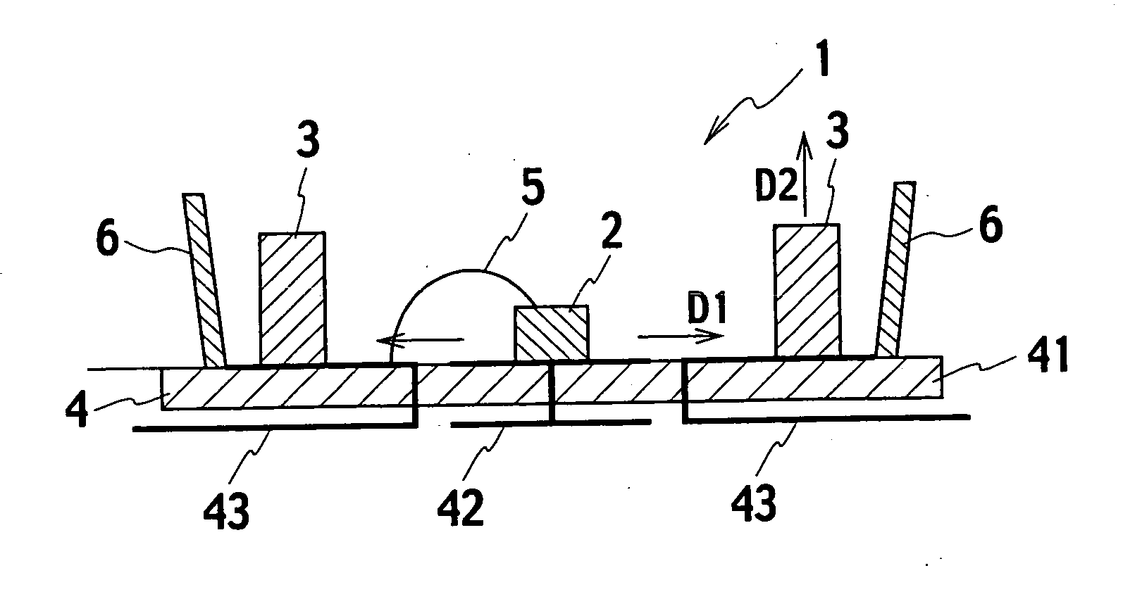
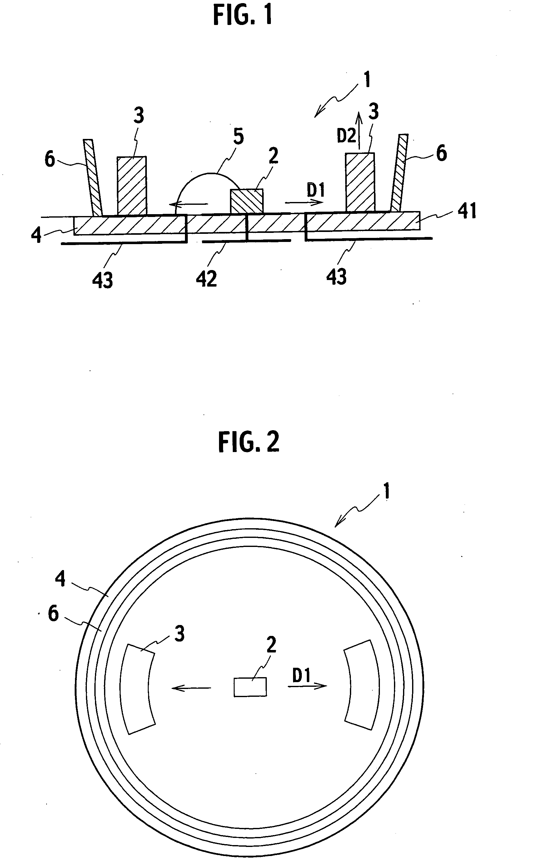
[0106] In the semiconductor light emitting device of the first embodiment, high energy excited light beams from the light emitting element 2 are disffused in the first direction D1 which is different from the second direction D2 where light beams from the fluorescent element 3 are received. All of the high energy light beams are absorbed by the fluorescent element 3 which is a wavelength conversion material. This enables the use of all of the high energy exciting light beams from the light emitting element 2, and allows the fluorescent element 3 to diffuse light beams having large outputs and high brightness.

[0107] The semiconductor light emitting device 1 has a simple structure which adjusts the direction of the high energy exciting light beams from the light emitting element 2 and the direction of light beams diffused by the fluorescent element 3. This is effective in reducing the number of components and in promoting downsizing.


PUM


Abstract

A semiconductor light emitting element includes a semiconductor light emitting element emitting light beams in ultraviolet ranges and visible ranges, and a fluorescent element absorbing the light beams from the semiconductor light emitting element and outputting visible light beams in a light taking-out direction different from a light emitting direction. The light beams emitted from the light emitting element is absorbed within the semiconductor light emitting device.

Description

CROSS REFERENCE TO RELATED APPLICATIONS [0001] This invention is based upon and claims the benefit of priority from prior Japanese Patent Application No. 2005-182,403 filed on Jun. 22, 2005; the entire contents of which are incorporated by reference herein. BACKGROUND OF THE INVENTION [0002] 1. Field of the Invention [0003] This invention relates to a semiconductor light emitting device, and more particularly relates to a semiconductor light emitting device including a semiconductor light emitting elements and a fluorescent element. [0004] 2. Description of the Related Art [0005] Japanese Patent Laid-Open Publication No. 2004-221,163 (called “Reference 1”) describes a light emitting device which can emit uniform light beams in an observing direction. The light emitting device includes not only a light emitting element but also light diffusing particulates which are provided on the light emitting element and diffuse light beams. Both of the light emitting element and light diffusing ...

Claims


Application Information

Patent Timeline
Patent Type & Authority Applications(United States)
IPC IPC(8): F21V7/04H01L33/28H01L33/32H01L33/44H01L33/50H01L33/54H01L33/56H01L33/60
CPCH01L33/505H01L33/507H01L33/60H01L2224/45144H01L2224/48091H01L2924/3025H01S5/183H01S5/32341H01S5/327H01S5/0087H01S5/02255H01S5/02315H01S5/02325H01S5/0239H01L2924/00014H01L2924/00H01S5/0225
Inventor HATTORI, YASUSHISAITO, SHINJINUNOUE, SHINYAYAMAMOTOSHIDA, NAOMIKANEKO, KEIHATAKOSHI, GENICHI
Owner ALPAD CORP
Why Eureka
Try Eureka