Organic light emitting diode display

a light-emitting diode and organic technology, applied in the field of organic light-emitting diodes, can solve the problems of reducing the aperture ratio increasing the cost and size of the oled panel, and deteriorating brightness, so as to reduce the number of lines

Active Publication Date: 2007-01-04
LG DISPLAY CO LTD
View PDF10 Cites 194 Cited by
  • Summary
  • Abstract
  • Description
  • Claims
  • Application Information

AI Technical Summary

Benefits of technology

[0017] Accordingly, it is an object of the present invention to provide an OLED panel capable of reducing the number of lines and an OLED display device employing the OLED panel.

Problems solved by technology

Meanwhile, the above-mentioned OLED display device has the following problems.
However, such a large number of the power voltage supply lines reduces an aperture ratio of the OLED panel and deteriorates brightness.
It also can increase the cost and size of the OLED panel.

Method used


Image

  • Organic light emitting diode display
  • Organic light emitting diode display
  • Organic light emitting diode display

Examples


first embodiment

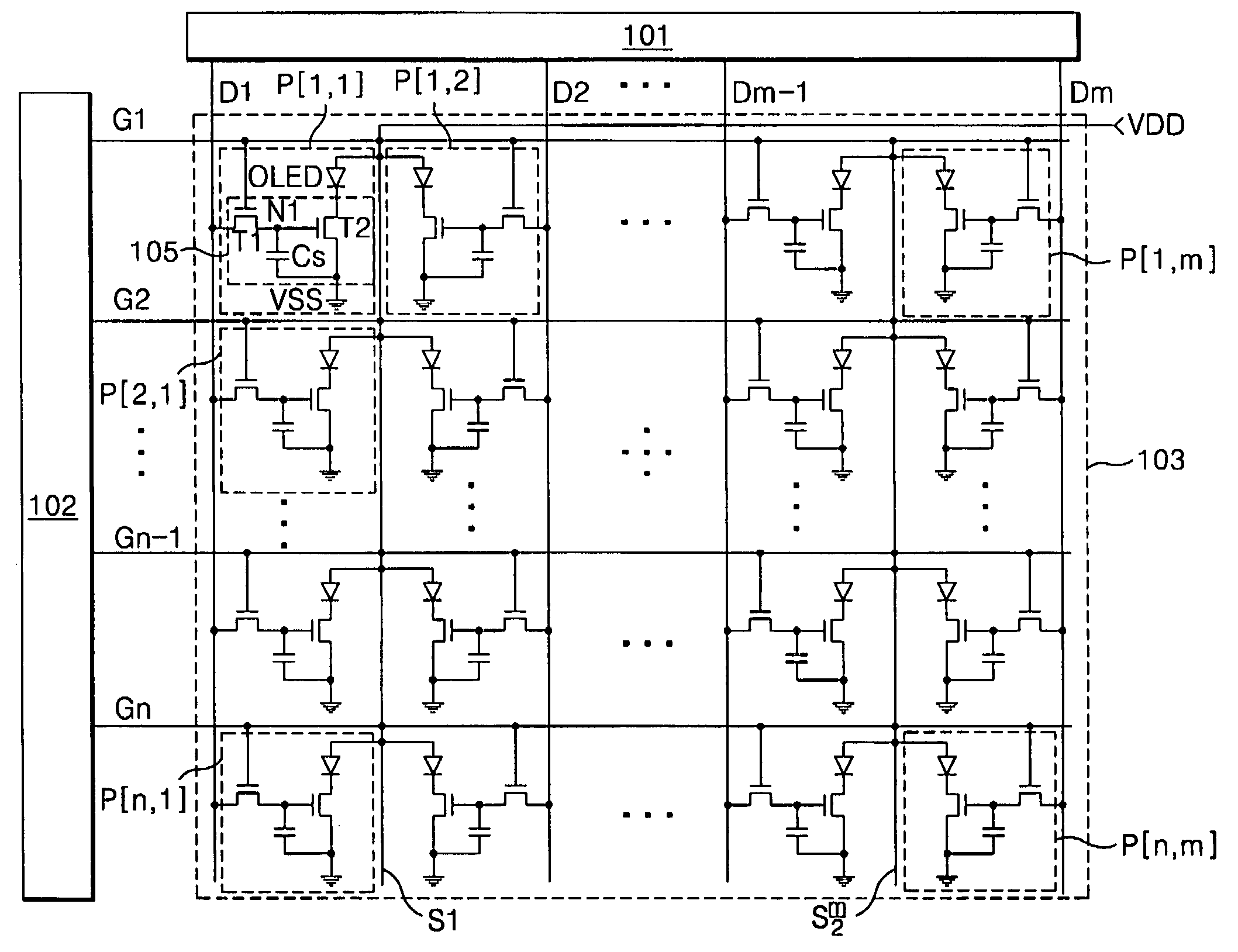
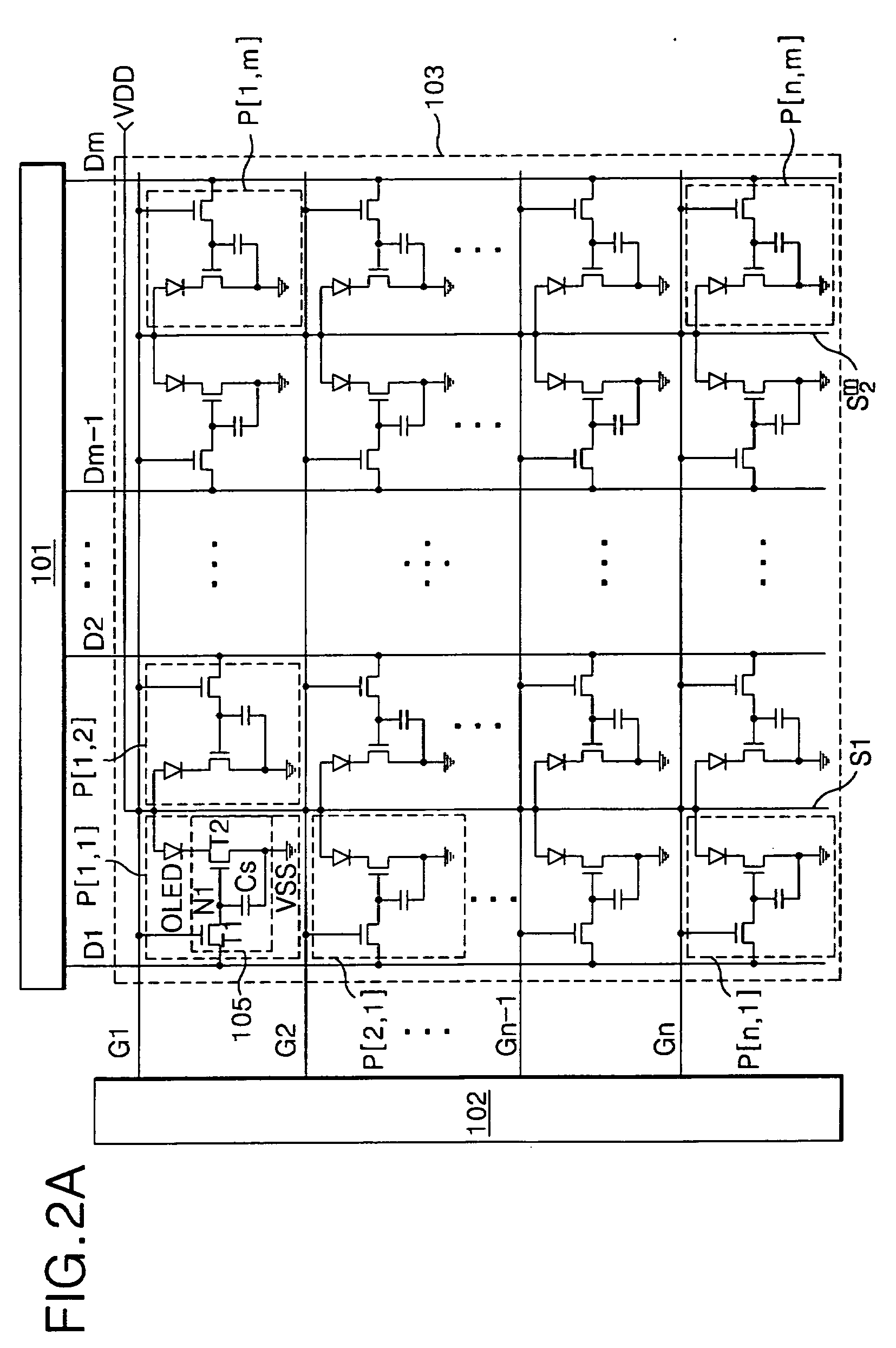
[0056] Referring to FIGS. 2A and 2B, an OLED display device according to the present invention includes an OLED panel 103 having n×m pixels P[i,j] arranged in a n×m matrix type at each area defined by n gate lines G1 to Gn, m data lines D1 to Dm, and m / 2 power voltage supply lines (wherein P[i,j] is a pixel positioned at an i row and a j column and wherein i is an integer smaller than or equal to n, and j is an integer smaller than or equal to m), a gate driving circuit 102 for driving the gate lines G1 to Gn of the OLED panel 103, and a data driving circuit 101 for driving the data lines D1 to Dm of the OLED panel 103. All the components of the OLED display device including the OLED panel 103 are operatively configured and coupled.

[0057] The gate driving circuit 102 supplies a scanning signal to the gate lines G1 to Gn to sequentially drive the gate lines G1 to Gn.

[0058] The data driving circuit 101 converts a digital data signal inputted from the exterior thereof into an analog d...

second embodiment

[0067]FIG. 3 shows a configuration of an organic light emitting diode display device according to the present invention.

[0068] Referring to FIG. 3, an OLED display device according to the second embodiment of the present invention includes an OLED panel 203 having n×m pixels P[i,j] arranged in a n×m matrix type at each area defined by n gate lines G1 to Gn, m data lines D1 to Dm, m / 2 power voltage supply lines S1 to Sm / 2 and n reset lines R1 to Rn for supplying a reset signal to each pixel P[i,j], a gate driving circuit 202 for driving the gate lines G1 to Gn of the OLED panel 203, and a data driving circuit 201 and a reset driving circuit 206 for driving the data lines D1 to Dm of the OLED panel 203. All the components of the OLED display device including the OLED panel 203 are operatively configured and coupled.

[0069] The gate driving circuit 202 supplies a scanning signal to the gate lines G1 to Gn to sequentially drive the gate lines G1 to Gn.

[0070] The data driving circuit 20...

third embodiment

[0089]FIG. 6 shows a configuration of an organic light emitting diode display device according to the present invention.

[0090] Referring to FIG. 6, an OLED display device according to the third embodiment of the present invention includes an OLED panel 303 having n×m pixels P[i,j] arranged in a n×m matrix type at each area defined by n gate lines G1 to Gn, m data lines D1 to Dm, m / 2 power voltage supply lines S1 to Sm / 2, n / 2 reset lines R1 to Rn / 2, a gate driving circuit 302 for driving the gate lines G1 to Gn of the OLED panel 303, a data driving circuit 301 for driving the data lines D1 to Dm of the OLED panel 303, and a reset driving circuit 306. Here P[i,j] is a pixel positioned at an i row and a j column, whereas i is an integer smaller than or equal to n, and j is an integer smaller than or equal to m. All the components of the OLED display device including the OLED panel 303 are operatively configured and coupled.

[0091] The gate driving circuit 302 supplies a scanning signal...


PUM


Abstract

An organic light emitting diode (OLED) display device for reducing the number of lines of an organic light emitting diode panel is provided. The OLED display device includes first and second data lines; a power voltage supply line supplied with a power supply voltage; a gate line crossing the first data line, the second data line and the power voltage supply line; first and second organic light emitting diodes commonly connected to the power voltage supply line; a first organic light emitting diode driving circuit for driving the first organic light emitting diode with a data voltage from the first data line in response to a scanning signal from the gate line; and a second organic light emitting diode driving circuit for driving the second organic light emitting diode with a data voltage from the second data line in response to the scanning signal from the gate line.

Description

[0001] This application claims the priority benefit of Korean Patent Application No. 10-2005-0058029 filed in Korea on Jun. 30, 2005, which is hereby incorporated by reference. BACKGROUND OF THE INVENTION [0002] 1. Field of the Invention [0003] This invention relates to an organic light emitting diode, and more particularly to an organic light emitting diode display device that is adaptive for reducing the number of power lines in an organic light emitting diode panel to thereby increase the aperture ratio of the display device as well as improve brightness. [0004] 2. Description of the Related Art [0005] Recently, there have been highlighted various flat panel display devices reduced in weight and bulk that are capable of eliminating disadvantages of a cathode ray tube (CRT). Such flat panel display devices include a liquid crystal display (LCD), a field emission display (FED), a plasma display panel (PDP) and a light emitting diode (LED) display, etc. [0006] The LED display device...

Claims


Application Information

Patent Timeline
Patent Type & Authority Applications(United States)
IPC IPC(8): G09G3/30H05B44/00
CPCG09G3/3233G09G3/3266G09G3/3291H01L27/3276G09G2310/0251G09G2320/043G09G2300/0465H10K59/131H05B33/26G09G3/30
Inventor PARK, KWON SHIKYOON, SOO YOUNGCHUN, MIN DOO
Owner LG DISPLAY CO LTD
Why Eureka
Try Eureka