

Fin field effect transistors (FinFETs) and methods for making the same
a technology of field effect transistor and finfet, which is applied in the field of sineconductor devices, can solve the problems of limited ability to tailor the structure of sineconductor resulting from such conventional methods
- Summary
- Abstract
- Description
- Claims
- Application Information
AI Technical Summary
Benefits of technology
Problems solved by technology
Method used
Image

Examples
Embodiment Construction
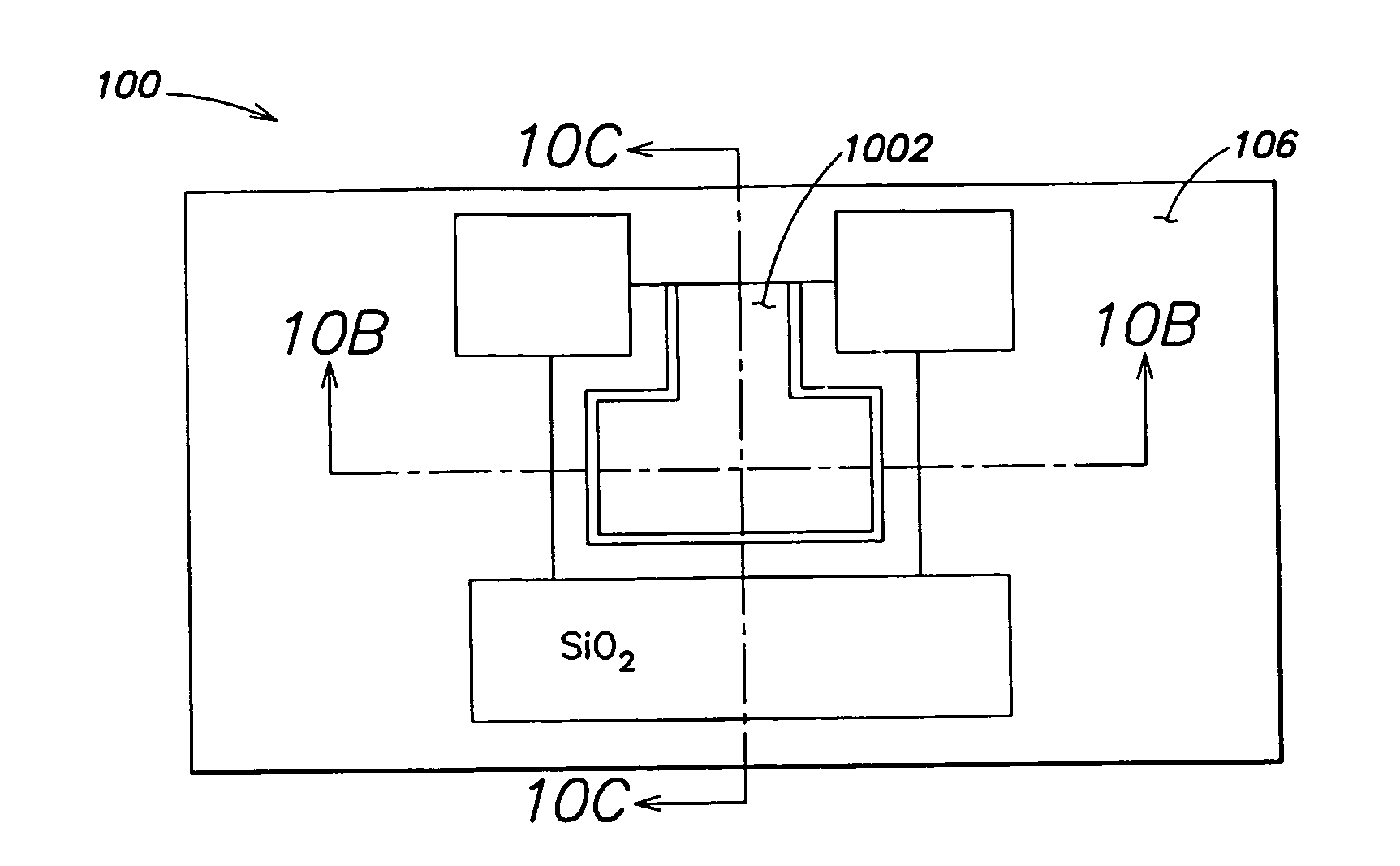
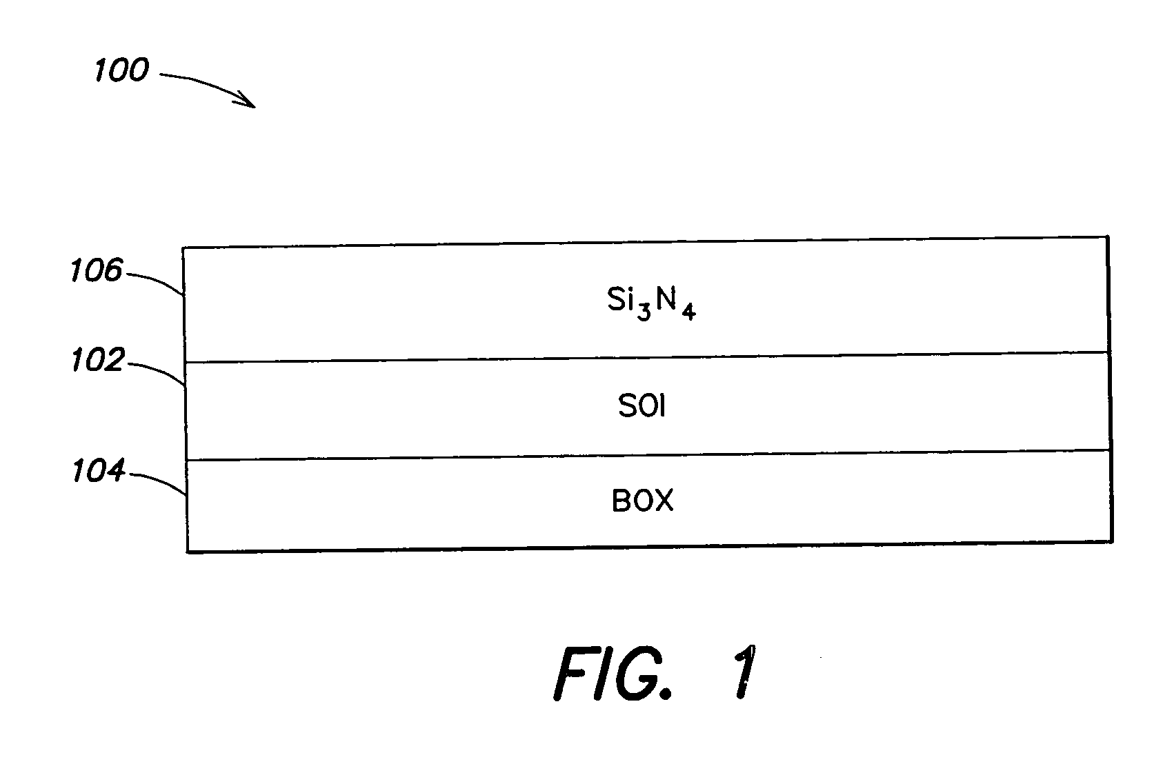
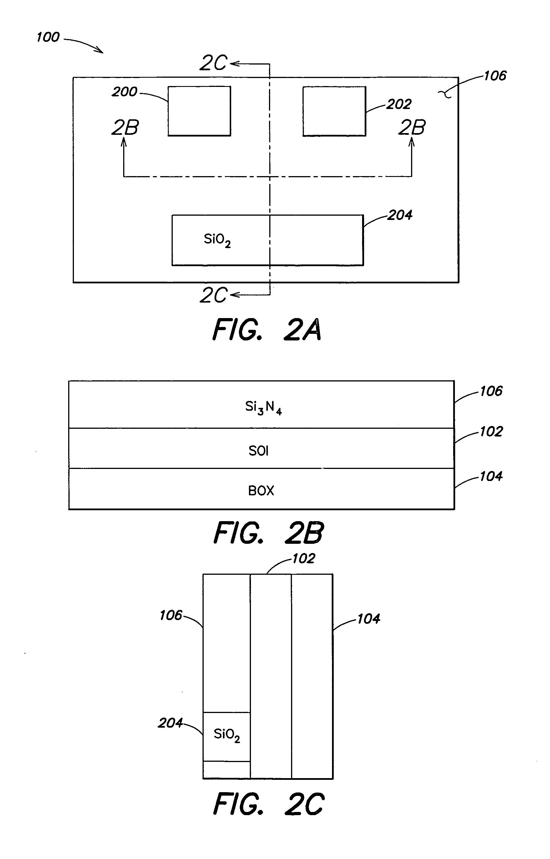
[0048] The present invention provides improved semiconductor devices and methods for making the same. More specifically, the present invention provides improved fin field effect transistors (FinFETS) and methods for making the same. The present methods of manufacturing FinFETs provide support (e.g., on one or more sides) to silicon which ultimately forms a fin during (e.g., throughout) manufacturing. In this manner, damage to the fin while manufacturing a FinFET may be reduced and / or eliminated, and therefore, a semiconductor device manufacturing yield may be improved.
[0049] Further, in contrast to conventional methods, the variability of a structure of a FinFET resulting from the present methods is not limited. For example, a FinFET in accordance with the present methods and apparatus may include a first gate conductor, which has a first work function, coupled to a first gate of the FinFET, and may include a second gate conductor, which has a different (e.g., a second) work functi...
PUM
 Abstract
Description
Claims
Application Information