Method of forming a MOS device having a strained channel region

a technology of metal oxidesemiconductor and channel region, which is applied in the direction of semiconductor devices, electrical equipment, transistors, etc., can solve the problems of limiting the strain that can be applied by the capping layer, the thickness of the strained capping layer is limited, and the constant effort of the vlsi circuit scaling, etc., to achieve the effect of improving the strain in the mos device without increasing the thickness of the contact etch stop layer

Inactive Publication Date: 2007-01-11
TAIWAN SEMICON MFG CO LTD
View PDF27 Cites 55 Cited by
  • Summary
  • Abstract
  • Description
  • Claims
  • Application Information

AI Technical Summary

Benefits of technology

[0014] The preferred embodiments of the present invention have the advantageous feature of impro

Problems solved by technology

The scaling of VLSI circuits is a constant effort.
The conventional methods of creating strain cause a dilemma.
However, the thickness of the strained capping layer is limited due

Method used


Image

  • Method of forming a MOS device having a strained channel region
  • Method of forming a MOS device having a strained channel region
  • Method of forming a MOS device having a strained channel region

Examples


Embodiment Construction

[0019] The making and using of the presently preferred embodiments are discussed in detail below. It should be appreciated, however, that the present invention provides many applicable inventive concepts that can be embodied in a wide variety of specific contexts. The specific embodiments discussed are merely illustrative of specific ways to make and use the invention, and do not limit the scope of the invention.

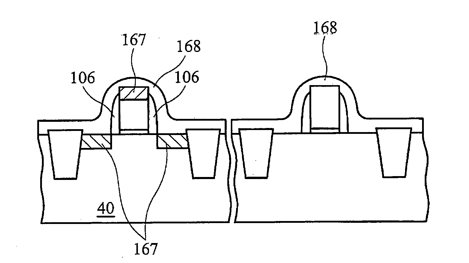
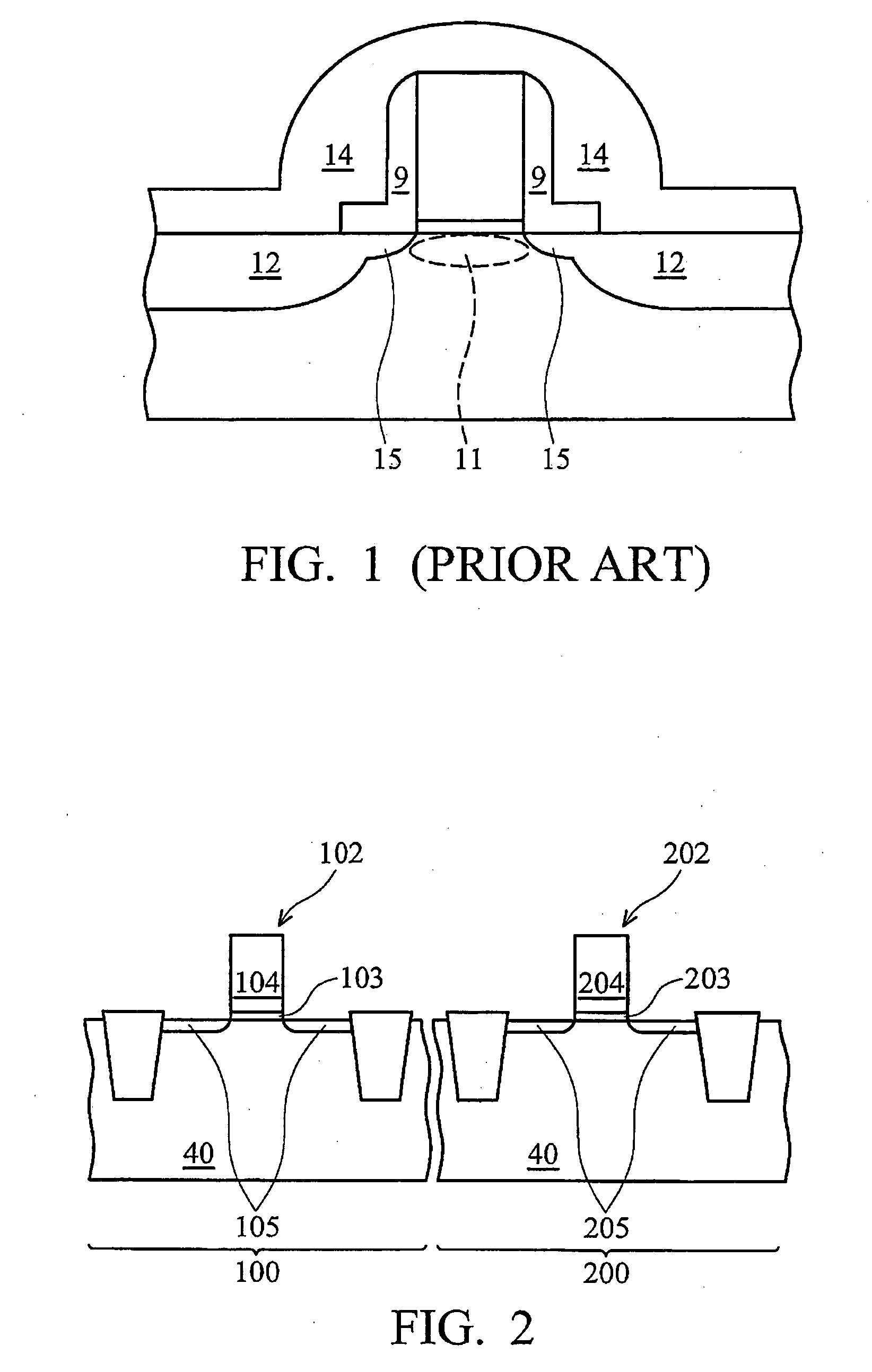
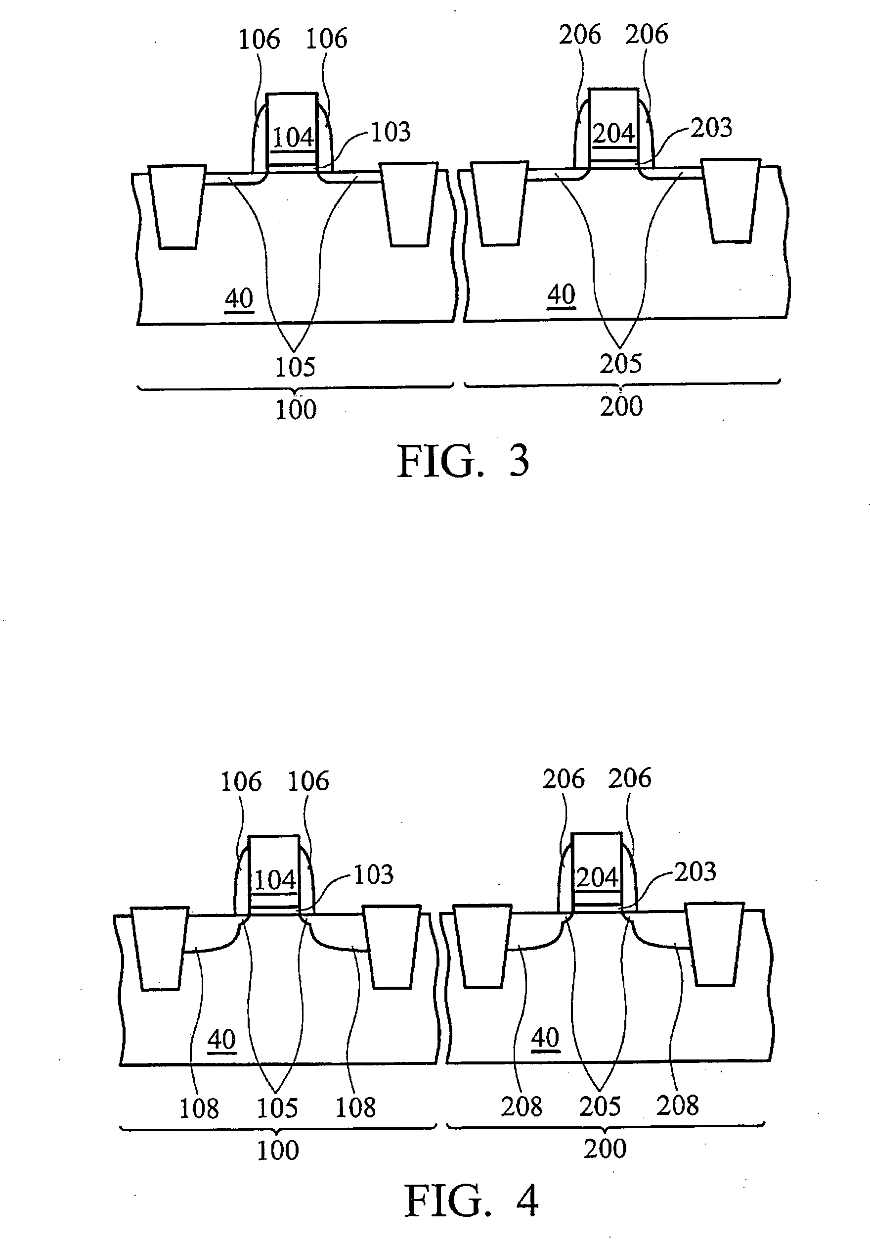
[0020] The preferred embodiments of the present invention are illustrated in FIGS. 2 through 9. Variations of the preferred embodiments are then discussed with reference to FIGS. 10 through 12. Throughout the various views and illustrative embodiments of the present invention, like reference numbers are used to designate like elements.

[0021] Referring to FIG. 2, a substrate 40 is provided. The substrate 40 can be formed of common substrate materials such as silicon, SiGe, strained silicon on SiGe, silicon on insulator (SOI), silicon germanium on insulator (SGOI), germanium...


PUM


Abstract

A method of forming a semiconductor device comprising providing a substrate comprising a first device region, implanting a source/drain region in the first device region, forming a strained capping layer on the source/drain region, super annealing and crystallizing the source/drain region, and removing substantially all of the strained capping layer is provided. The method further includes pre-amorphizing the source/drain region before the super annealing. The strained capping layer may further be formed on a pre-amorphized gate electrode, and the gate electrode is super annealed. The strain is generated and preserved after the removal of the strained capping layer.

Description

TECHNICAL FIELD [0001] This invention relates generally to metal-oxide-semiconductor (MOS) devices, and more particularly to MOS devices with strained channel regions and processes for forming the same. BACKGROUND [0002] The scaling of VLSI circuits is a constant effort. With circuits becoming smaller and faster, device driving current improvement is becoming more important. Device current is closely related to gate length, gate capacitance, and carrier mobility. Shortening poly-gate length, increasing gate capacitance, and increasing carrier mobility can improve the device current performance. Gate length reduction is an on-going effort to shrink circuit size. Increased gate capacitance has been achieved by efforts such as reducing the thickness of the gate dielectric, increasing the gate dielectric constant, and the like. In order to further improve device current, the enhancement of carrier mobility has also been explored. [0003] Among efforts made to enhance carrier mobility, fo...

Claims


Application Information

Patent Timeline
IPC IPC(8): H01L21/20H01L21/4763
CPCH01L21/26506H01L21/324H01L21/76828H01L21/76829H01L21/823412H01L29/7843H01L21/823807H01L21/823842H01L29/6659H01L29/7833H01L21/82345
Inventor CHEN, CHIEN-HAONIEH, CHUN-FENGLEE, TZE-LIANGCHEN, SHIH-CHANGLIANG, MONG SONG
Owner TAIWAN SEMICON MFG CO LTD
Why Eureka
Try Eureka