Integrated circuit device and electronic instrument

a technology of integrated circuits and electronic instruments, applied in the field of integrated circuit devices and electronic instruments, can solve the problems of increasing circuit scale and circuit complexity, reducing the chip area of the driver circuit, and manufacturing costs that cannot be reduced

Inactive Publication Date: 2007-01-18
138 EAST LCD ADVANCEMENTS LTD
View PDF74 Cites 32 Cited by
  • Summary
  • Abstract
  • Description
  • Claims
  • Application Information

AI Technical Summary

Benefits of technology

[0009] wherein a second power supply interconnect for supplying a second power supply voltage to the memory cells is provided in a metal

Problems solved by technology

However, since many types of circuits are necessary for a high-performance driver circuit, the circuit scale and the circuit complexity tend to be increased in proportion to an increase in resolution of a display panel.
Therefore, since it is difficult to reduce the chip area of the driver circuit while maintaining the high performance or providing a

Method used


Image

  • Integrated circuit device and electronic instrument
  • Integrated circuit device and electronic instrument
  • Integrated circuit device and electronic instrument

Examples


embodiment

5. Effect of Embodiment

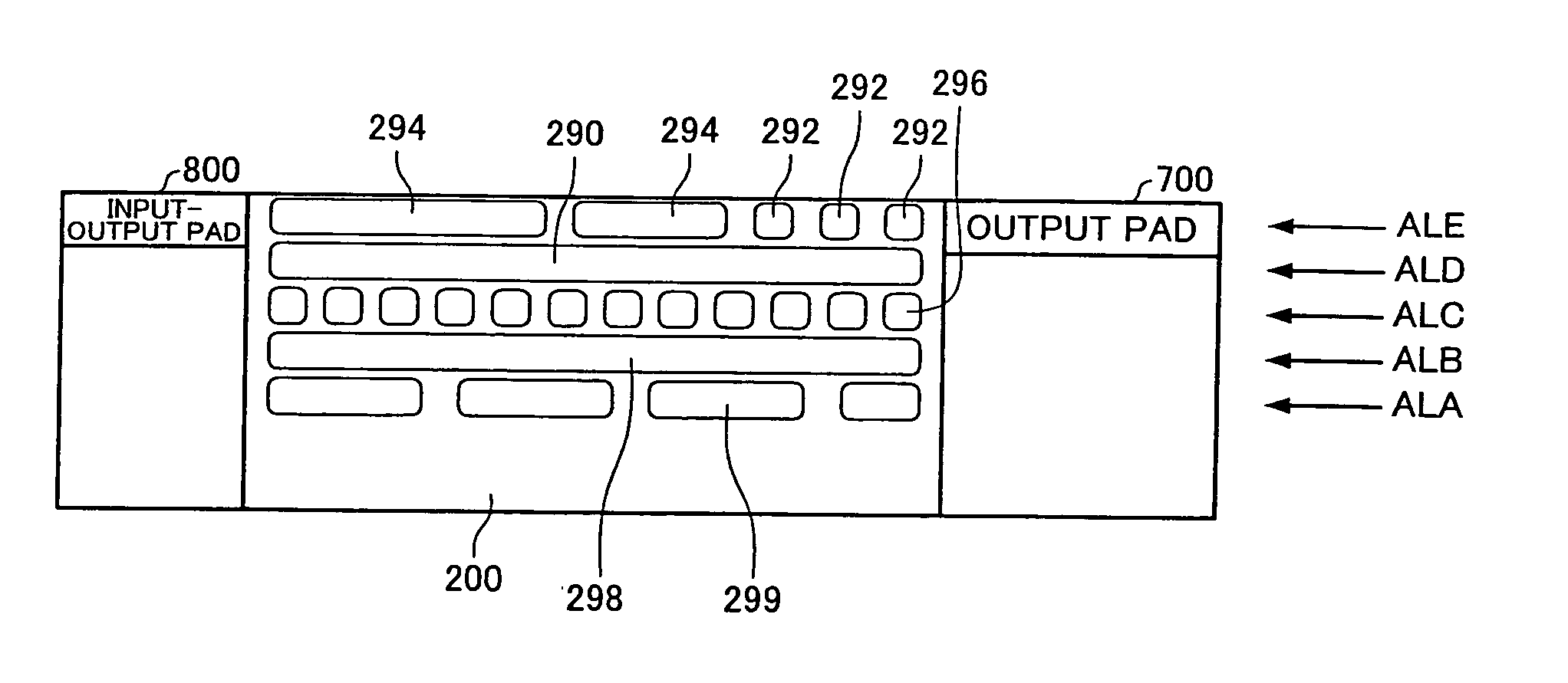
[0255] In the embodiment, the shield interconnects SHD2 are formed in the RAM 200 as shown in FIGS. 19, 20, 21, and 24. This enables normal data detection even if the third power supply interconnect GL is formed in the upper layer of the bitlines BL and / BL. Therefore, since various interconnects can be formed in the upper layer of the RAM 200, the circuit blocks of the display driver 20 can be flexibly arranged. For example, the grayscale voltage necessary for the data line driver 100 (circuit other than the display memory in a broad sense) can be supplied through the upper layer of the RAM 200. Specifically, a layout in which the chip area of the display driver 20 is minimized can be achieved, whereby manufacturing cost is reduced.

[0256] The shield interconnect SHD2 is formed along the direction X as shown in FIGS. 19, 20, 21, and 24. Therefore, the shield interconnect SHD2 can be used as a power supply interconnect for supplying the voltage VSS, whereby a ...


PUM


Abstract

An integrated circuit device having a display memory, wherein a plurality of first power supply interconnects for supplying a first power supply voltage to a plurality of memory cells are provided in a metal interconnect layer in which a plurality of bitlines are formed; wherein a second power supply interconnect for supplying a second power supply voltage to the memory cells is provided in a metal interconnect layer in which a plurality of wordlines are formed, the second power supply voltage being higher than the first power supply voltage; wherein a plurality of bitline protection interconnects are formed in a layer above the bitlines, each of the bitline protection interconnects at least partially covering one of the bitlines in a plan view; and wherein a third power supply interconnect for supplying a third power supply voltage to circuits of the integrated circuit device other than the display memory is provided in a layer above the bitline protection interconnects, the third power supply voltage being higher than the second power supply voltage.

Description

[0001] Japanese Patent Application No. 2005-192952, filed on Jun. 30, 2005, is hereby incorporated by reference in its entirety. BACKGROUND OF THE INVENTION [0002] The present invention relates to an integrated circuit device and an electronic instrument. [0003] In recent years, an increase in resolution of a display panel provided in an electronic instrument has been demanded accompanying a widespread use of electronic instruments. Therefore, a driver circuit which drives a display panel is required to have high performance. However, since many types of circuits are necessary for a high-performance driver circuit, the circuit scale and the circuit complexity tend to be increased in proportion to an increase in resolution of a display panel. Therefore, since it is difficult to reduce the chip area of the driver circuit while maintaining the high performance or providing an additional function, manufacturing cost cannot be reduced. [0004] A high-resolution display panel is also provi...

Claims


Application Information

Patent Timeline
IPC IPC(8): H01L23/52
CPCG11C5/063H01L23/552H01L2224/49175H01L2924/14H01L2924/01066H01L2924/3025H01L24/49H01L2924/01019H01L2924/01037H01L2924/19041H01L2924/00014H01L2224/45099G09G3/20G11C7/18
Inventor KODAIRA, SATORUITOMI, NOBORUKAWAGUCHI, SHUJIKUMAGAI, TAKASHIISHIYAMA, HISANOBUMAEKAWA, KAZUHIRO
Owner 138 EAST LCD ADVANCEMENTS LTD
Why Eureka
Try Eureka