Analog amplifier having DC offset cancellation circuit and method of offset cancellation for analog amplifiers

an analog amplifier and offset cancellation technology, applied in the field of analog amplifier offset cancellation schemes, can solve the problems of sensitivity reduction, dc offset producing mismatch in the common mode voltage of differential outputs of amplifiers, asymmetry or mismatching of amplifier components,

Active Publication Date: 2007-01-18
AVAGO TECH INT SALES PTE LTD
View PDF24 Cites 33 Cited by
  • Summary
  • Abstract
  • Description
  • Claims
  • Application Information

AI Technical Summary

Problems solved by technology

This offset causes asymmetry or mismatching of the amplifier components.
Of particular note, the DC offset produces mismatch in the common mode voltages of the differential outputs of the amplifier.
When the offset voltage is higher, the decision circuit will slice the data at a non-optimal level which leads to a sensitivity reduction and thus a poor bit-error-rate performance.
This undesired effect leads to a low frequency cutoff in the main amplifier 12's frequency response.
As a result, the resistance and capacitance used in the RC network are usually very large, occupying excessive and often unacceptable amounts of chip area.

Method used


Image

  • Analog amplifier having DC offset cancellation circuit and method of offset cancellation for analog amplifiers
  • Analog amplifier having DC offset cancellation circuit and method of offset cancellation for analog amplifiers
  • Analog amplifier having DC offset cancellation circuit and method of offset cancellation for analog amplifiers

Examples


Embodiment Construction

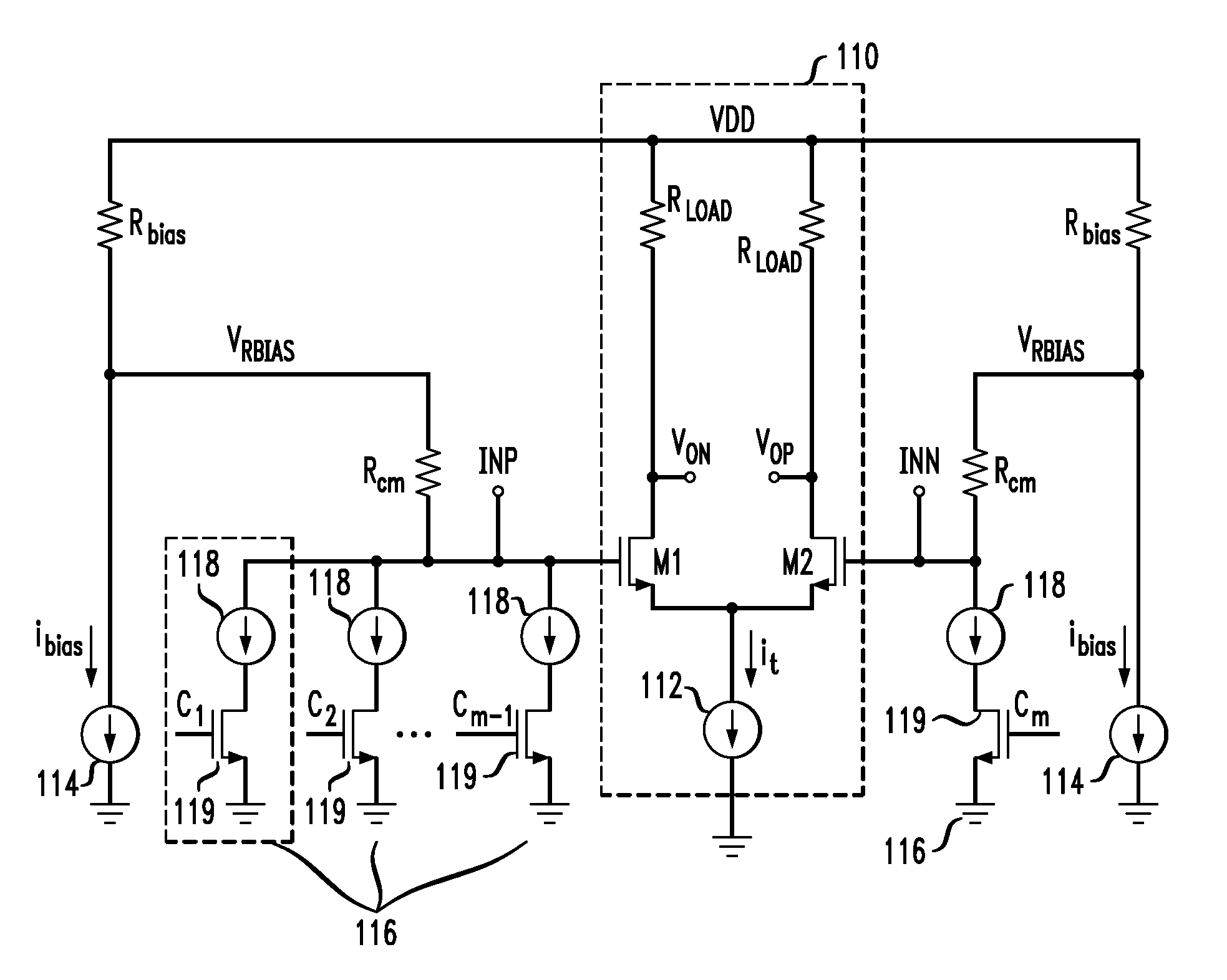
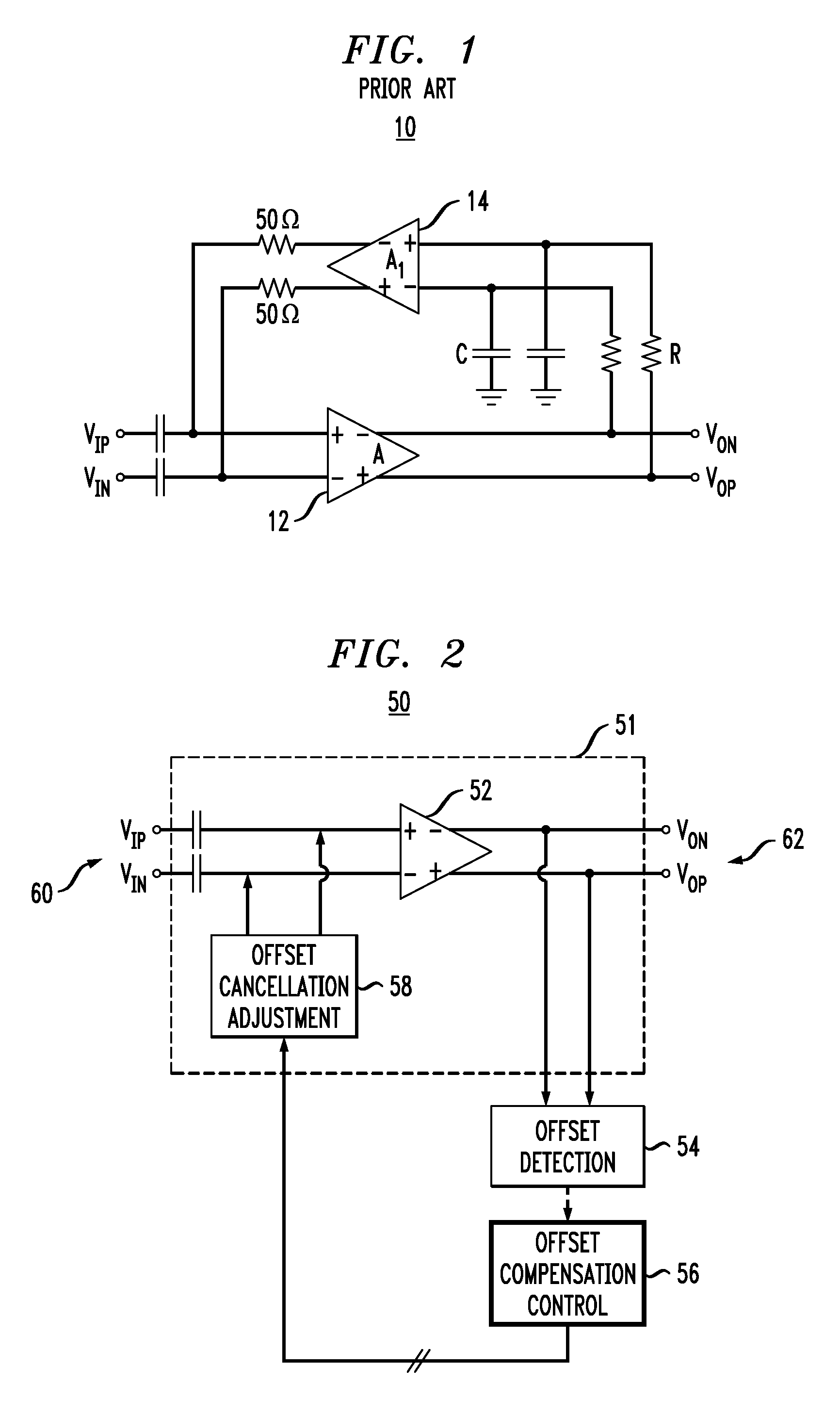
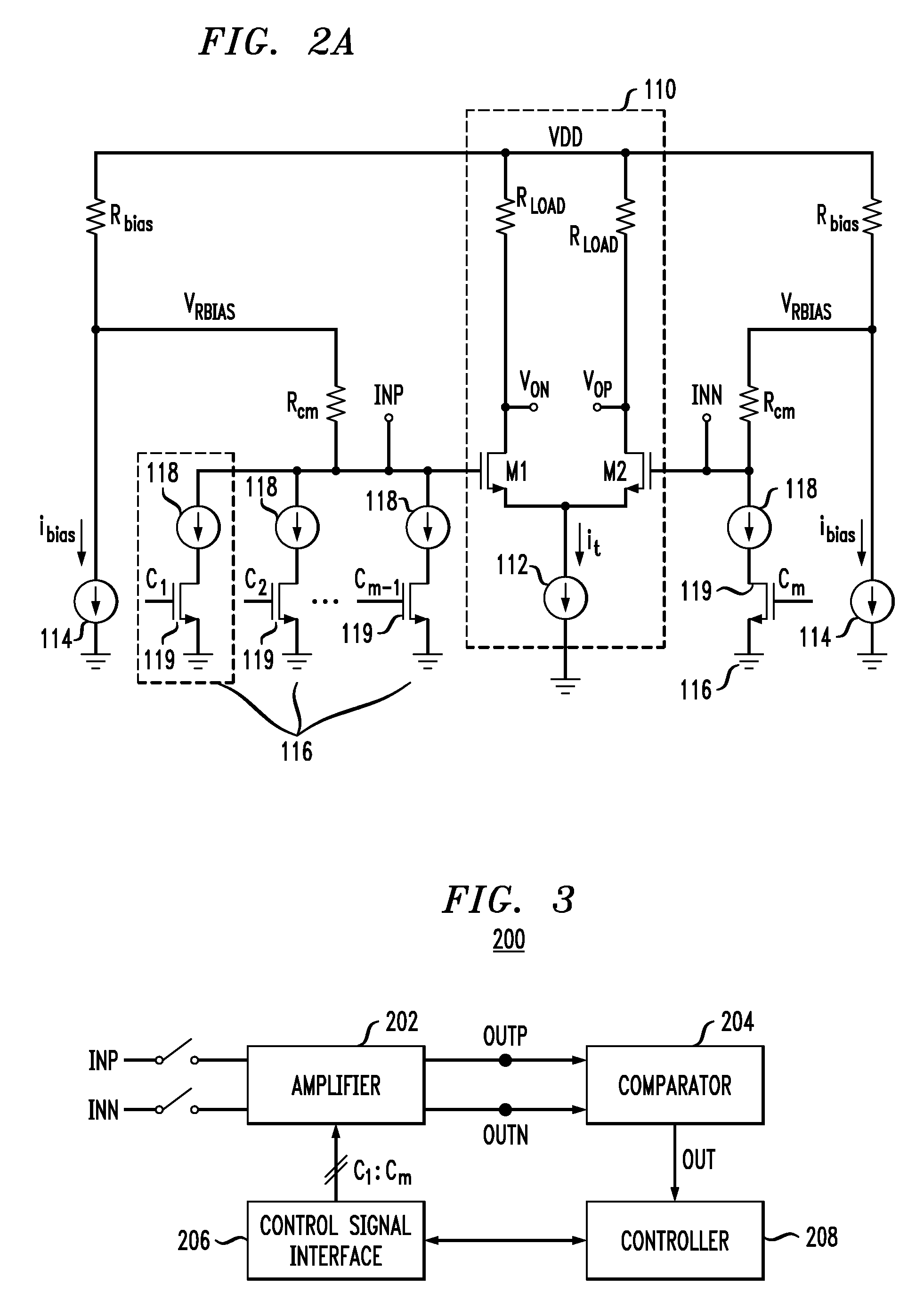
[0016]FIG. 2 is a block diagram of a system 50 for detecting and compensation for DC offset in an analog amplifier. The system includes an analog amplifier 51 having offset cancellation adjustment circuitry 58, an offset detection module 54 and an offset compensation control module 56. In one embodiment, the components shown within shadow box 51 are integrated on a single chip or substrate to form an amplifier, while offset detection module and offset compensation control modules 54, 56 are used for calibration of the amplifier 51 as described below in more detail. Though shown as separate components, offset detection module 54 and / or offset compensation control module 56 may be integrated into a chip or substrate with amplifier 51 to form a feedback loop in a self-calibrating amplifier. In one embodiment, only offset detection module 54 is integrated with amplifier device 51.

[0017] The amplifier device 51 of FIG. 2 includes inputs for receiving an input data signal 60. The input d...


PUM


Abstract

An amplifier having DC offset compensation includes at least one input node and a pair of differential output nodes, a biasing circuit coupled to the input node; and a plurality of current sources. Selected ones of said current sources are coupled to the input node to adjust a DC voltage at the input node to provide DC offset compensation for the amplifier

Description

CROSS-REFERENCE TO RELATED APPLICATION [0001] This application claims priority to U.S. Provisional Patent Application Ser. No. 60 / 698,375 filed Jul. 12, 2005 and entitled “Electrical Backplane Equalization Using Programmable Analog Zeros And Folded Active Inductors”, the entirety of which is hereby incorporated by reference herein.FIELD OF THE INVENTION [0002] The present invention relates generally to analog amplifiers and more particularly to offset cancellation schemes for analog amplifiers. BACKGROUND OF THE INVENTION [0003] Differential amplifiers typically have a built-in or internal DC offset due to device mismatch and parameter variations caused by manufacturing variations, as will be understood by those in the art. This offset causes asymmetry or mismatching of the amplifier components. Of particular note, the DC offset produces mismatch in the common mode voltages of the differential outputs of the amplifier. The input-referred offset voltage of an amplifier is the differe...

Claims


Application Information

Patent Timeline
Patent Type & Authority Applications(United States)
IPC IPC(8): H03F1/02
CPCH03F3/45973H03F3/45977H03F2203/45101H03F2203/45622H03F2203/45564H03F2203/45588H03F2203/45434
Inventor CHEN, JINGHONGSHEETS, GREGORYANIDJAR, JOSEPHKAPUSCHINSKY, ROBERTSMITH, LANE
Owner AVAGO TECH INT SALES PTE LTD
Why Eureka
Try Eureka