Sub-mount for mounting optical component and light transmission and reception module

a technology for optical components and sub-mounts, applied in the direction of instruments, optical elements, optical waveguide light guides, etc., can solve the problem of large mounting cos

Inactive Publication Date: 2007-01-18
FUJIFILM BUSINESS INNOVATION CORP
View PDF9 Cites 20 Cited by
  • Summary
  • Abstract
  • Description
  • Claims
  • Application Information

AI Technical Summary

Problems solved by technology

However, the methods proposed so far requires a mirror to be embedded to form a 90° return mirror, and requires positioning at high precision when laminating the waveguide and the light transmission and reception element, and thus the cost required for mounting becomes large.

Method used


Image

  • Sub-mount for mounting optical component and light transmission and reception module
  • Sub-mount for mounting optical component and light transmission and reception module
  • Sub-mount for mounting optical component and light transmission and reception module

Examples


example 1

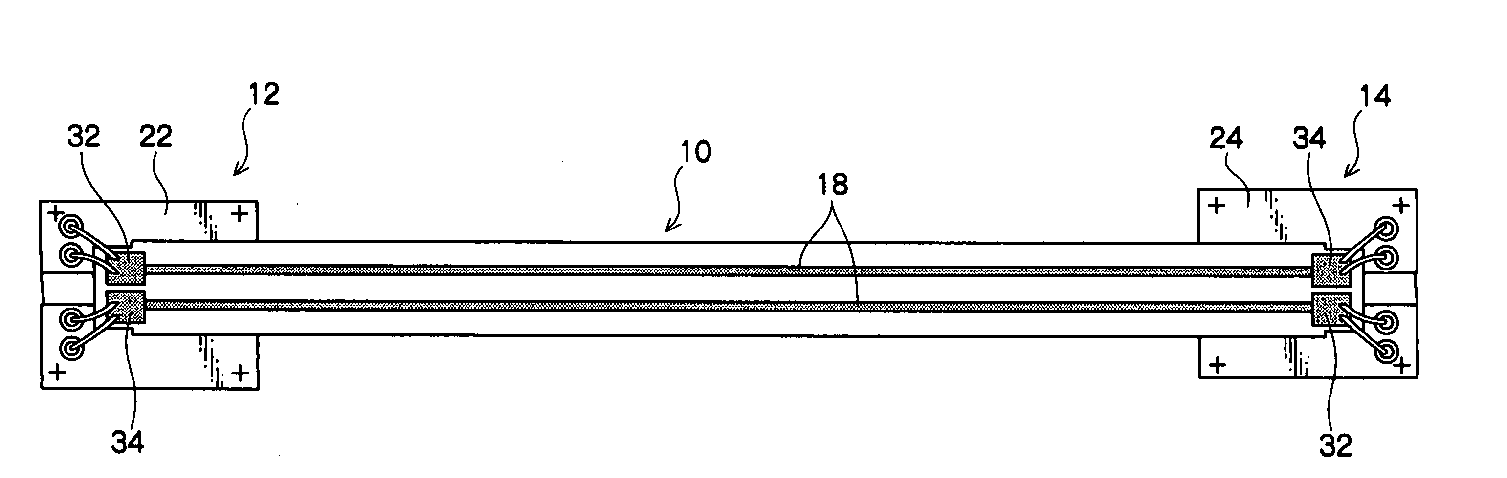
[0150] Sub-mounts are produced with “Duplication Method using Silicone Resin” and the light transmission and reception module shown in FIG. 3 is produced.

[0151] (Production of Polymer Optical Waveguide Film)

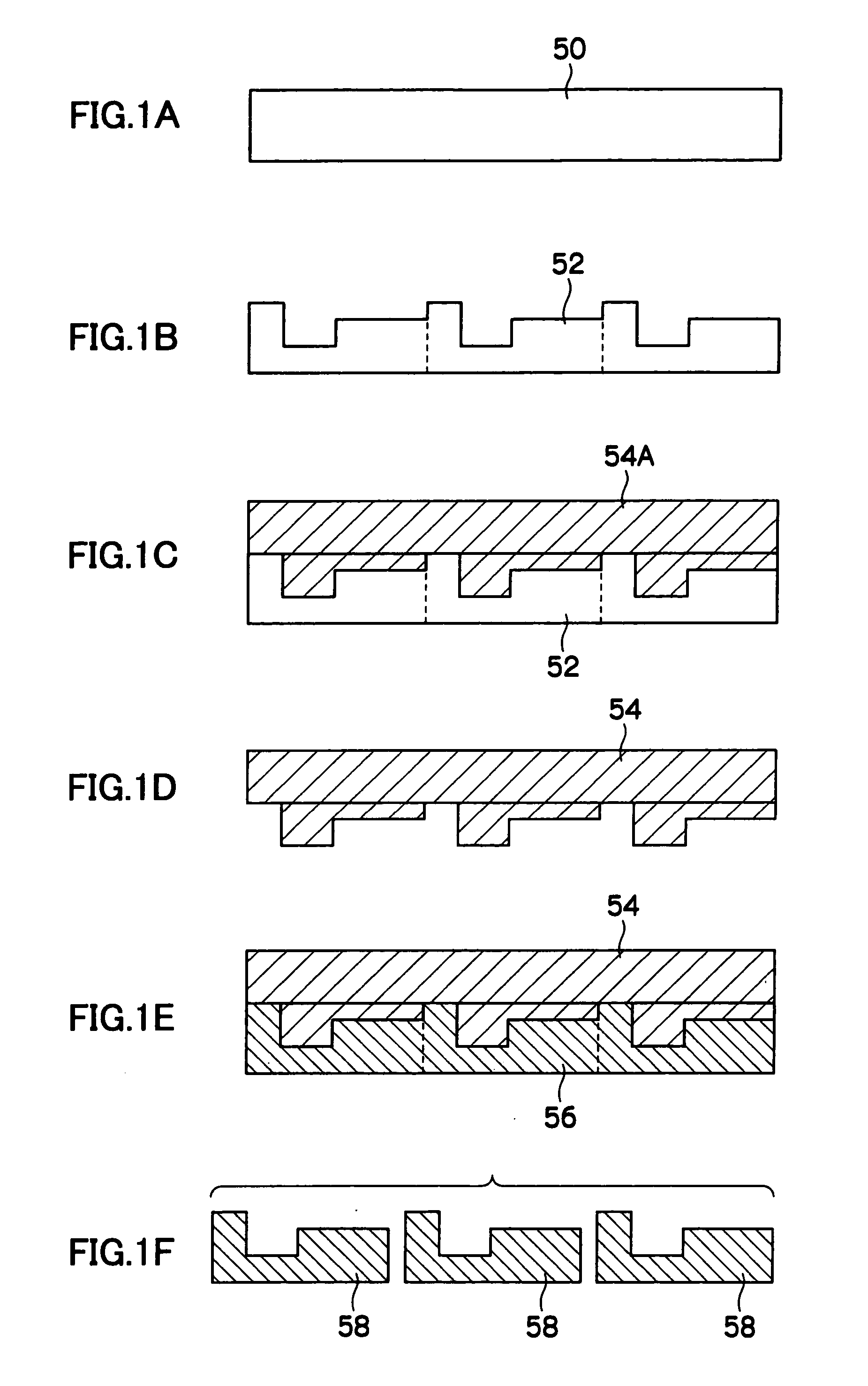
[0152] After an Si substrate is coated with a thick film resist (trade name: SU-8, manufactured by Microchemical) according to a spin coat method, it is prebaked at 80 deg. C., is exposed through a photomask and is developed so that four projections having a quadrate section (width: 50 μm, height: 50 μm, length: 80 mm) are formed. Each gap between the projections is set to 250 μm. The Si substrate coated with the thick film resist is post-baked at 120 deg. C., so that a master plate for manufacturing a polymer waveguide is produced.

[0153] A releasing agent is applied on the master plate, and a mixture of thermosetting liquid dimethyl siloxane rubber (product name: SYLGARD184 manufactured by Dow-Corning Asia, viscosity 5000 mPa.s) and its hardening agent is poured in, and heate...

example 2

[0169] The sub-mount made of resin is produced through “Stamper Method”, and the light transmission and reception module shown in FIG. 3 is produced. The light transmission and reception module is produced using the method similar to Example 1 except that producing the sub-mount with “Stamper Method”.

[0170] (Production of Sub-Mount)

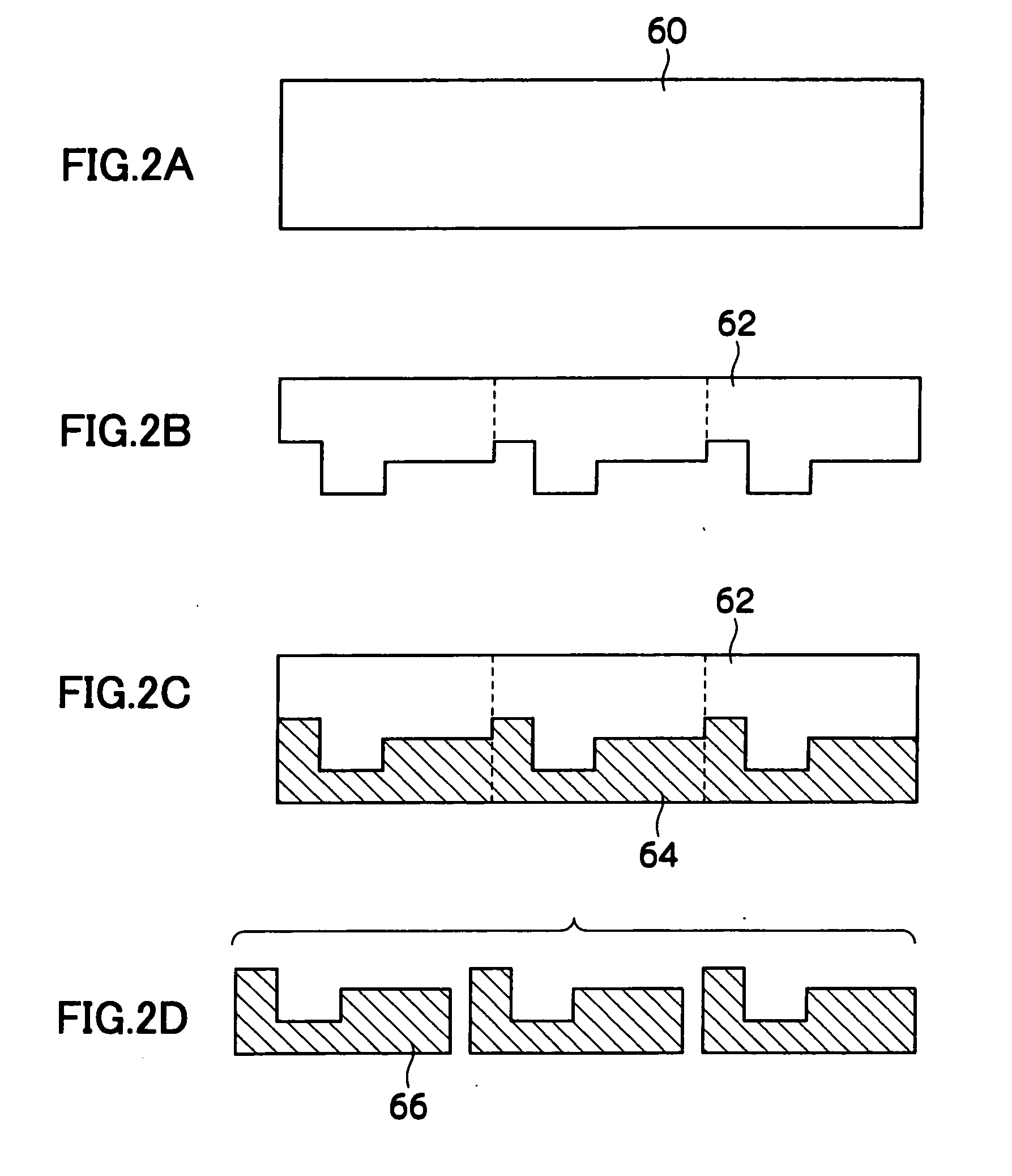
[0171] The master substrate made of Si is produced similar to Example 1. The master substrate is used as the stamper (mold) and the thermoplastic bulk molding compound (BMC) resin is adhered to the stamper, heated for two minutes under a pressure of 100 N and at a temperature of 250 deg. C., and thereafter, stood to cool to cure the epoxy resin. The cured layer is then stripped from the stamper, thereby producing the cured resin layer (thickness of mold: 5 mm), which surface includes projections and recesses corresponding to the projections and recesses of the stamper.

[0172] Next, after vapor depositing Au on the cured resin layer at a thickness of 200...

example 3

[0178] A sub-mount made of glass is produced through “Stamper Method”, and the light transmission and reception module shown in FIG. 3 is produced. The light transmission and reception module is produced using the method similar to Example 2 except that producing the sub-mount made of glass through “Stamper Method” using a metal die, as explained below.

[0179] (Production of Sub-Mount)

[0180] A die (a master substrate) made of Ni including a recess having a depth of 250 μm for mounting the light emitting element and the light detecing element, and a recess having a depth of 50 μm for mounting the polymer waveguide film is molded. Using the die as the stamper (mold), low melting glass (made from Sumita Optical Glass Inc., “K-PG375” (Vidron), Tg: 343 deg. C., Yielding point: 363 deg. C.) is adhered to the stamper, heated for five minutes under a pressure of 10 Pa and at a temperature of 375 deg. C., and thereafter stood to cool to cure the low melting glass. The cured glass layer is t...


PUM


Abstract

A sub-mount includes a recess for holding a polymer optical waveguide film and recesses for embedding and holding a light emitting element and a light detecting element. The sub-mount further has an adhesive filling groove formed adjacent to respective recesses. When mounting the polymer optical waveguide film, the light emitting element, and the light detecting element onto the sub-mount, an adhesive is accurately applied and is prevented from flowing out as the adhesive filling grooves are provided.

Description

CROSS-REFERENCE TO RELATED APPLICATION [0001] This application claims priority under 35 USC 119 from Japanese patent document, No. 2005-207178, the disclosure of which is incorporated by reference herein. BACKGROUND OF THE INVENTION [0002] 1. Field of the Invention [0003] The present invention relates to a sub-mount and to a light transmission and reception module, more specifically, to a sub-mount mounted in a package of an optical device and to a light transmission and reception module using the same. [0004] 2. Description of the Related Art [0005] Recently, in IC technique or LSI technique, optical wiring between equipments, between boards in the equipments, or in a chip is given attention instead of the electrical wiring at high density to enhance the operating speed or integration degree. [0006] In Japanese Patent Application Laid-Open No. 2000-39530, for example, an optical element including a light emitting element and a light detecting element in a core clad stacking directi...

Claims


Application Information

Patent Timeline
Patent Type & Authority Applications(United States)
IPC IPC(8): G02B6/36G02B6/38
CPCG02B6/1221G02B6/4203G02B6/4246G02B6/43H01L2224/45144H01L2224/48091H01L2924/00014H01L2924/00
Inventor OHTSU, SHIGEMISUZUKI, TOSHIHIKOSHIMIZU, KEISHIFUJII, AKIRAYATSUDA, KAZUTOSHIAKUTSU, EIICHI
Owner FUJIFILM BUSINESS INNOVATION CORP
Why Eureka
Try Eureka