Method and apparatus for semiconductor processing

a technology of semiconductors and processing methods, applied in the direction of coatings, metallic material coating processes, chemical vapor deposition coatings, etc., can solve the problems of increasing coo, limiting the throughput of processing sequences, and impracticality of potentially desirable processing sequences

Inactive Publication Date: 2007-01-25
APPLIED MATERIALS INC
View PDF34 Cites 142 Cited by
  • Summary
  • Abstract
  • Description
  • Claims
  • Application Information

AI Technical Summary

Problems solved by technology

If the substrate throughput in a integrated tool is not limited by robot availability, a long device fabrication step will limit the throughput of the processing sequence, increase the COO, and make a potentially desirable processing sequence impractical.
To meet these tighter process requirements, the industry has developed new processes, but they often take more time to complete.
When forced to use slower processes for improved device performance, the fabrication cost increases because of the slower substrate throughput.
Although it is possible to add more chambers to the integrated processing tool to meet the desired throughput, it is often impractical to increase the number of process chambers or tools without significantly increasing the size of a integrated processing tool and the staff to run the tools.
These are often the most expensive aspects of the substrate fabrication process.
If the substrate is exposed to the atmosphere or other sources of contaminants for longer than the acceptable queue time the device performance may be reduced because of contamination of the interface between the first and second layers.
Problems with current methods of forming metal oxide films over substrates include high surface roughness, high crystallinity, and / or poor nucleation of the formed metal oxide film.

Method used


Image

  • Method and apparatus for semiconductor processing
  • Method and apparatus for semiconductor processing
  • Method and apparatus for semiconductor processing

Examples


Embodiment Construction

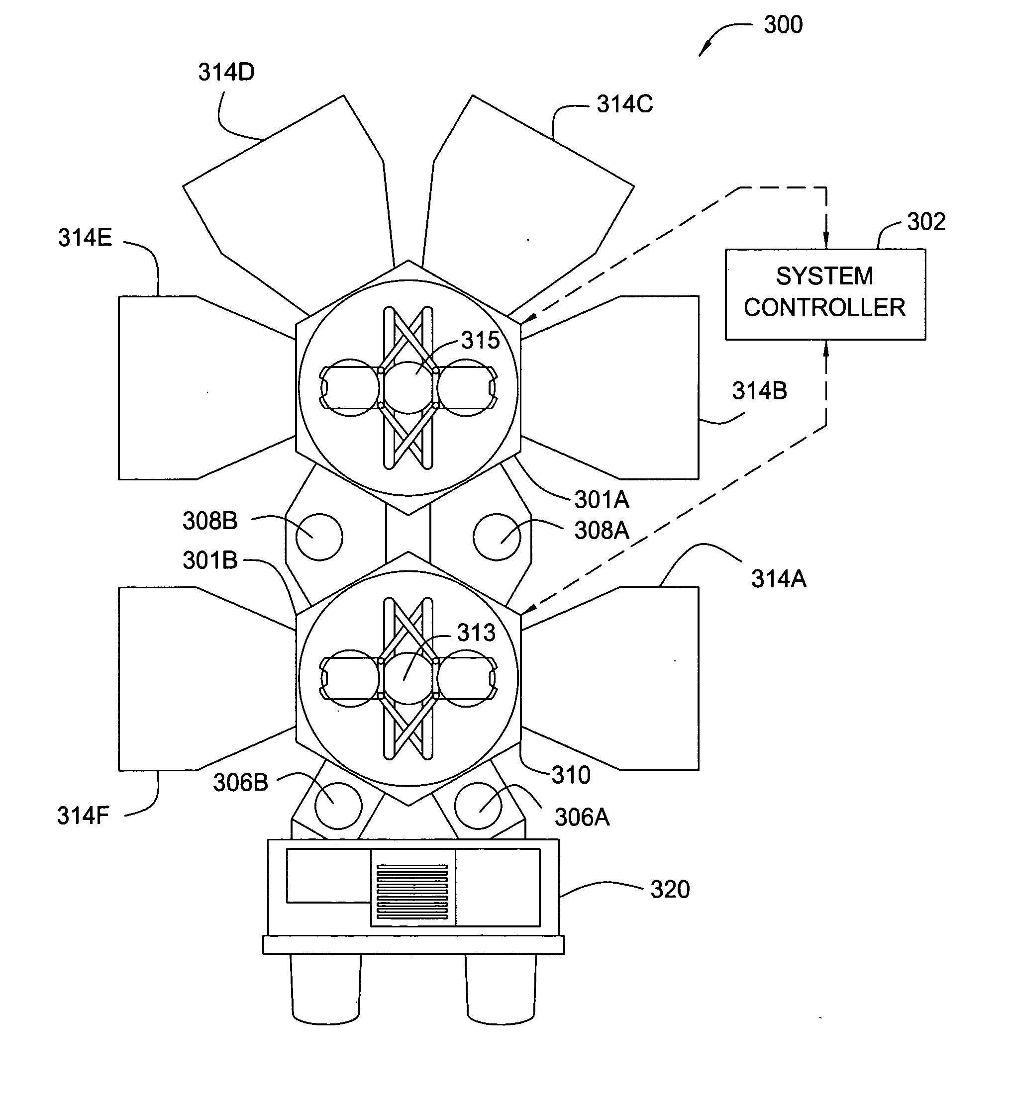
[0035] The present invention relates to an integrated processing tool configured to perform extended processing sequences by combining two or ore processing tools.

Processing Tools

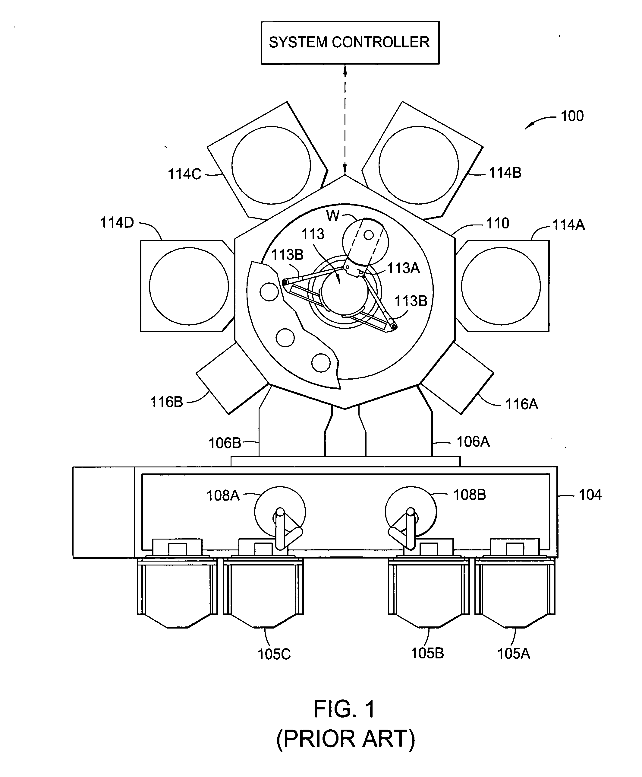
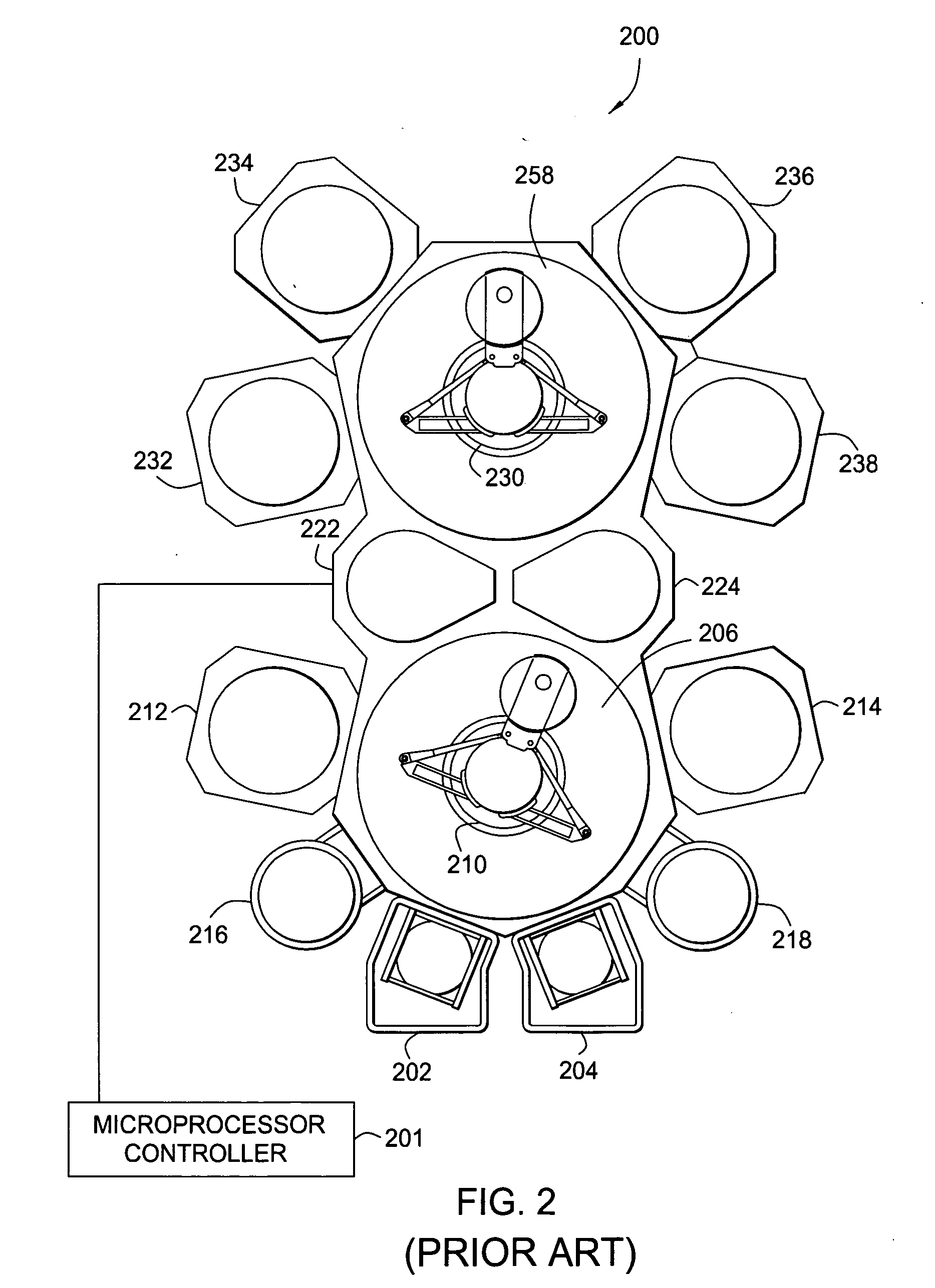
[0036]FIGS. 1 and 2 provide embodiments of available processing tools wherein the exact arrangement and combination of processing chambers may be altered for performing specific steps of a fabrication process. However, the total number of processing chambers is limited by several factors including the exterior surface area of the interior chamber for attaching the interchangeable process chambers. That is, interior chamber dimensions have to be selected to balance providing interchangeable process chambers, conserving floor space, and configuring the robots to reach within the interior portions of chambers and the load lock chambers. Also, service chambers may be attached to the exterior surface area of interior chamber.

Integrated Processing Tools with 5 or More Process Chambers

[0037]FIG. 3 is a schem...


PUM

PropertyMeasurementUnit
pressureaaaaaaaaaa
dielectric constantaaaaaaaaaa
temperatureaaaaaaaaaa

Abstract

A method and apparatus for manufacturing semiconductors, comprising at least two transfer chambers with exterior walls, at least one holding chamber attached to the transfer chamber, at least one load lock chamber attached to the walls of the transfer chambers, and at least five process chambers attached to the walls of the transfer chambers. A method and apparatus of depositing a high dielectric constant film, comprising depositing a base oxide on a substrate in a first process chamber, providing decoupled plasma nitration to a surface of the substrate in at least one second process chamber, annealing the surface of the substrate in a third process chamber, and depositing polycrystalline silicon in at least one forth process chamber, wherein the first, second, third, and fourth process chambers are in fluid communication with a common interior chamber.

Description

CROSS-REFERENCE TO RELATED APPLICATIONS [0001] This application claims benefit of U.S. Provisional Patent Application Ser. No. 60 / 700,523 (APPM / 010008L), filed Jul. 19, 2005, which is herein incorporated by reference.BACKGROUND OF THE INVENTION [0002] 1. Field of the Invention [0003] Embodiments of the invention generally relate to an integrated electronic device processing system configured to perform processing sequences with multiple deposition processing modules. [0004] 2. Description of the Related Art [0005] Semiconductor devices are formed by processing substrates in a multi-chamber processing system such as an integrated tool. Multiple chambers in communication with each other in a closed environment are desirable because it reduces chemical and particle contamination and avoids additional power consumption that would arise if the substrates are exposed to room air between chambers. The chambers are segregated by rigid walls, windows, slit valves, and other equipment to prot...

Claims


Application Information

Patent Timeline
Patent Type & Authority Applications(United States)
IPC IPC(8): H01L21/20C23C16/00
CPCH01L21/67207H01L21/67184H01L21/67
Inventor THAKUR, RANDHIRSPLINTER, MICHAEL
Owner APPLIED MATERIALS INC
Why Eureka
Try Eureka