Method of manufacturing thin-film electronic device

Active Publication Date: 2007-02-01
TDK CORPARATION
View PDF6 Cites 1 Cited by
  • Summary
  • Abstract
  • Description
  • Claims
  • Application Information

AI Technical Summary

Benefits of technology

[0007] On the other hand, a method of manufacturing a thin-film electronic device is an example of a method in which a through-hole is made after an electronic device has been produced on a substrate. When, for instance, an electrode layer having a certain pattern is provided on the front of the substrate, and a through-hole is then made from the back of the substrate so as to pass through the substrate and the electrode layer, it is likely for the material of the electrode layer to scatter. The scattered electrode material can adhere to the electrode

Problems solved by technology

Many problems are encountered when an electronic device is

Method used


Image

  • Method of manufacturing thin-film electronic device
  • Method of manufacturing thin-film electronic device
  • Method of manufacturing thin-film electronic device

Examples


Embodiment Construction

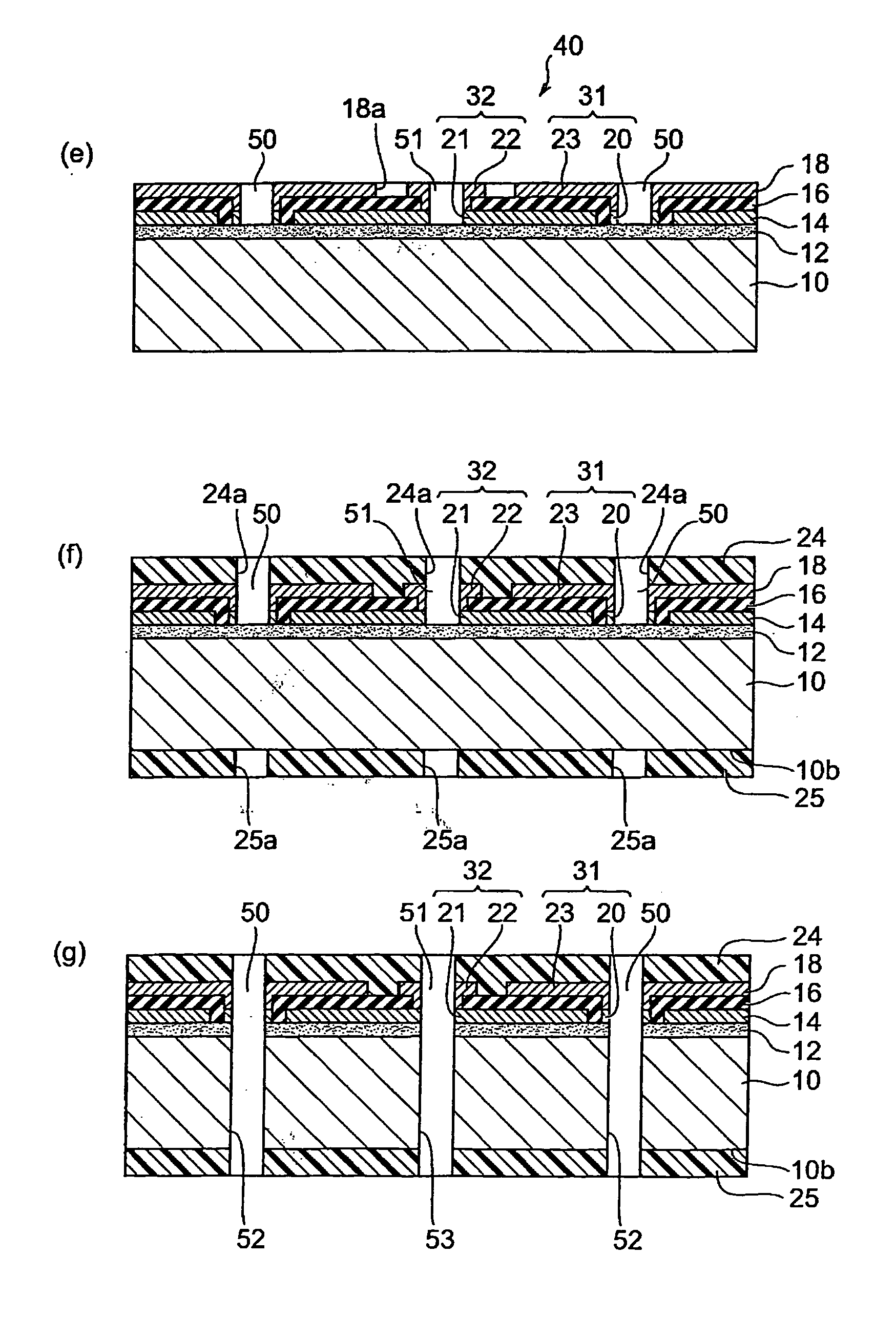
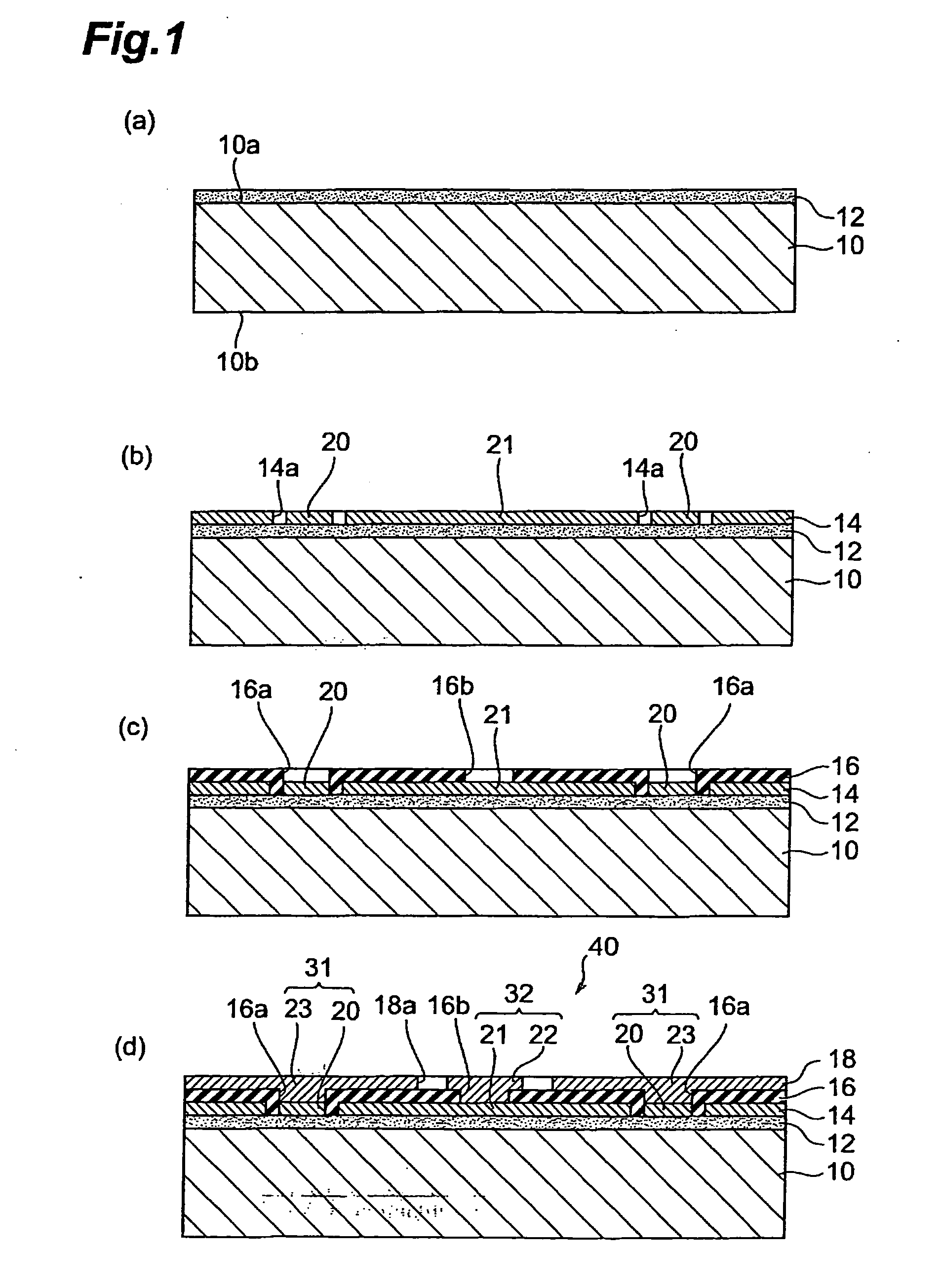
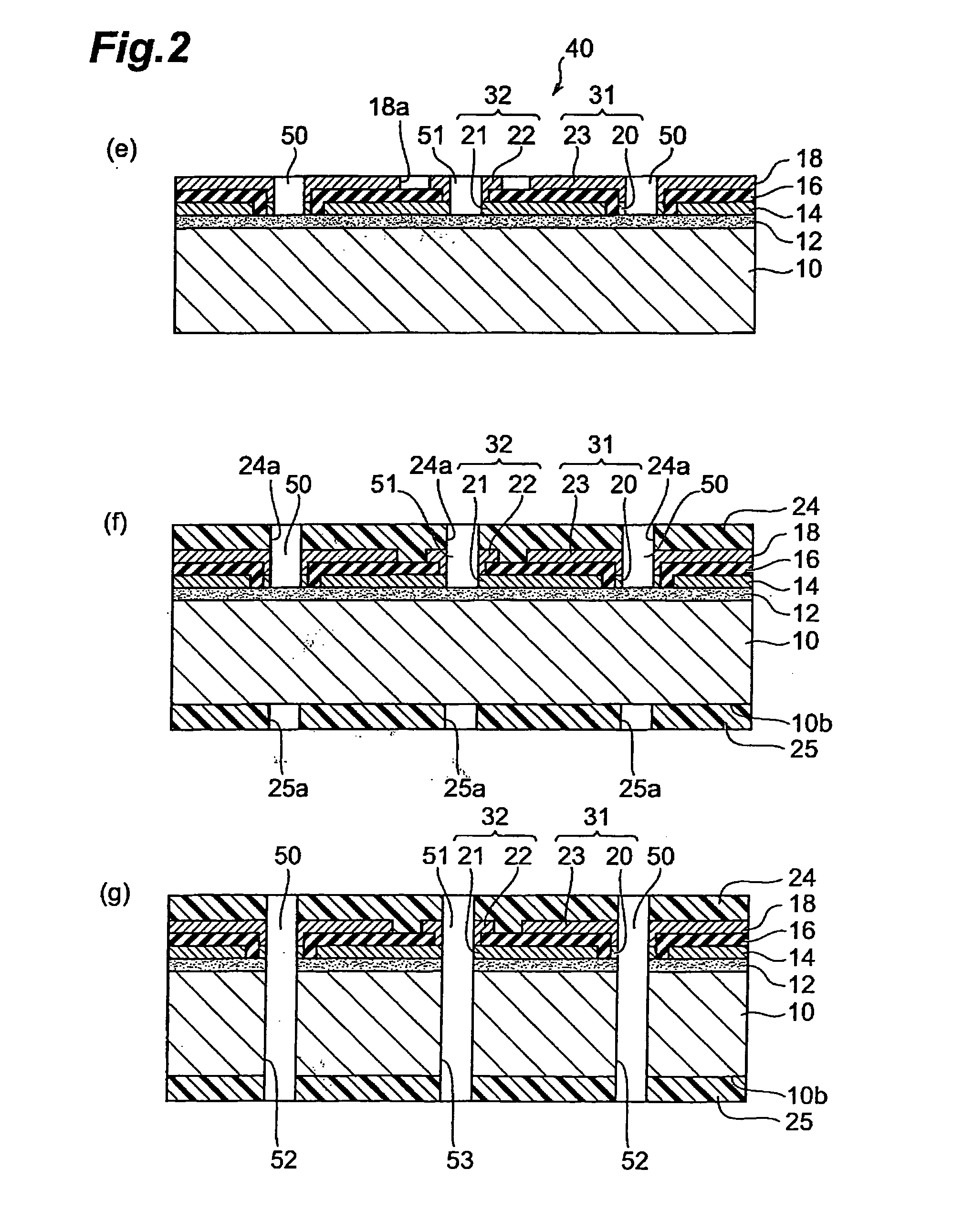
[0021] Embodiments of the present invention will now be described in detail with reference to the accompanying drawings. In the description of the drawings, identical symbols are used for identical elements, and these elements will not be explained repeatedly.

[0022] FIGS. 1 to 3 are schematic sectional views illustrating a method of manufacturing a thin-film electronic device in accordance with the embodiment. In this embodiment, a thin-film capacitor is manufactured as a thin-film electronic device. First, as shown in FIG. 1(a), a substrate 10 made of alumina is prepared, and one surface 10a of the substrate 10 is polished and planarized, and then this surface 10a is covered with an insulating film 12. The surface 10a of the substrate 10 is a face on which a thin-film capacitor is formed, and will hereinafter be called the front face. The other surface 10b of the substrate 10 will be called the back face. The insulating film 12 is made of SiO2 glass, and can be formed by plasma CV...


PUM


Abstract

A method of manufacturing a thin-film electronic device comprising providing a dielectric layer on a base, providing a first electrically conductive layer having a first opening and covering at least part of the dielectric layer; and forming a first through-hole extending through the base and communicating with the first opening. A second electrically conductive layer may be provided on the base, and a dielectric layer may be provided so as to cover at least part of this second conductive layer.

Description

BACKGROUND OF THE INVENTION [0001] 1. Field of the Invention [0002] The present invention relates to a method of manufacturing a thin-film electronic device. [0003] 2. Related Background Art [0004] Japanese Laid-Open Patent Applications H11-260148 and 2004-48045 each disclose a thin-film electronic device formed on a substrate having a through-hole. This through-hole is used to produce a via that electrically connects wiring on the front side of the substrate to wiring on the back side thereof, for example. As discussed in Japanese Laid-Open Patent Application H11-260148, a laser can be used to form the through-hole. SUMMARY OF THE INVENTION [0005] The production of a thin-film electronic device formed on a substrate having a through-hole can be roughly classified into two methods. One is a method in which the electronic device is produced after the through-hole has been made, and the other is a method in which the through-hole is made after the electronic device has been produced o...

Claims


Application Information

Patent Timeline
IPC IPC(8): H01L21/84
CPCH01L27/016
Inventor KOMURO, EIJUSHINOURA, OSAMUOZAKI, YUMIKOSHIBUE, AKIRA
Owner TDK CORPARATION
Why Eureka
Try Eureka