

Semiconductor device and method of manufacturing the same
a semiconductor and semiconductor technology, applied in the field of semiconductor devices, can solve the problems of increasing the manufacturing cost of semiconductor devices, and achieve the effects of increasing the manufacturing cost, high planarity, and high planarity
- Summary
- Abstract
- Description
- Claims
- Application Information
AI Technical Summary
Benefits of technology
Problems solved by technology
Method used
Image

Examples
Embodiment Construction
[0033] The invention will be now described herein with reference to illustrative embodiments. Those skilled in the art will recognize that many alternative embodiments can be accomplished using the teachings of the present invention and that the invention is not limited to the embodiments illustrated for explanatory purposes.
[0034] Hereunder, exemplary embodiments of a semiconductor device and a method of manufacturing the same according to the present invention will be described in details, referring to the accompanying drawings. In the drawings, same constituents are given the identical numerals, and duplicating description may be omitted where appropriate.
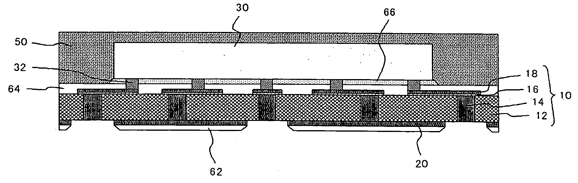
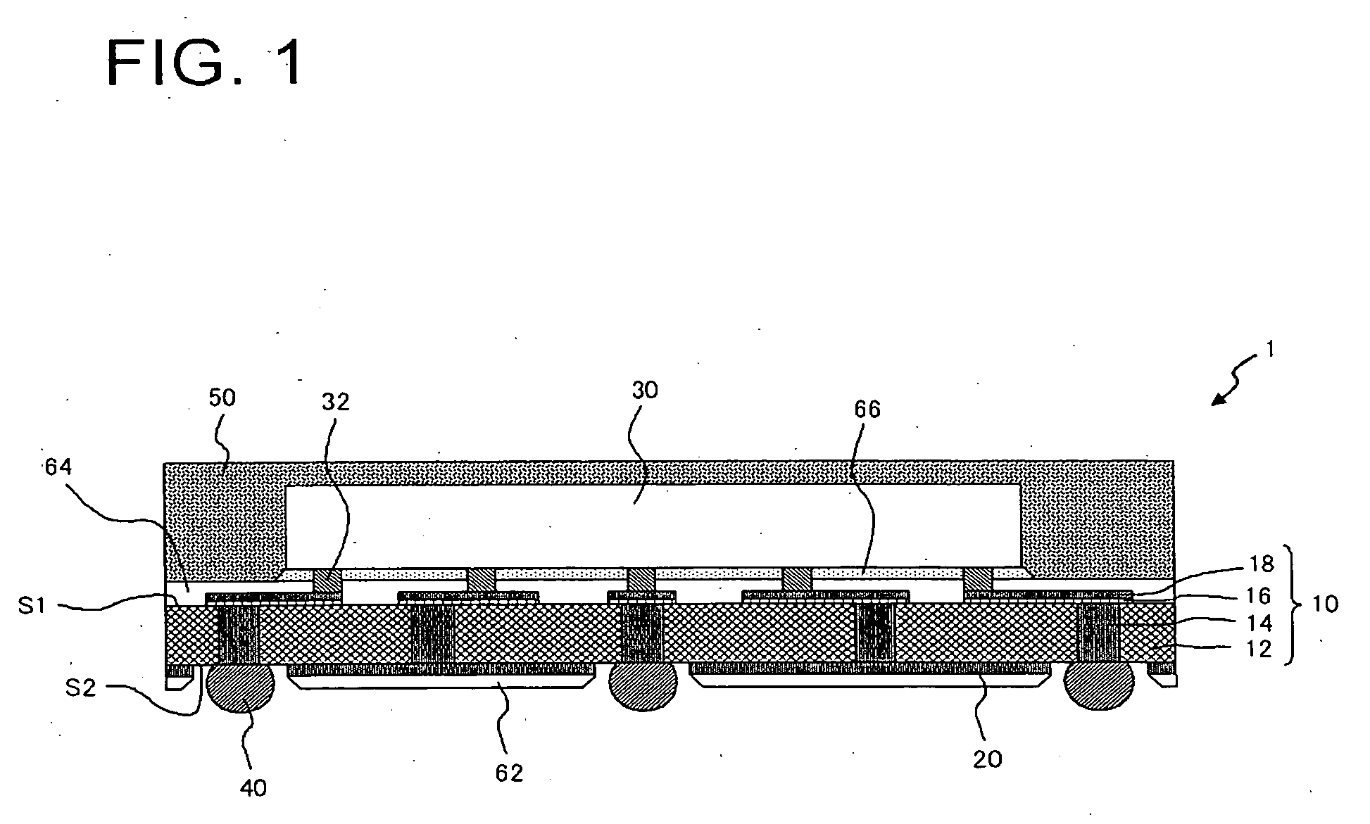
[0035]FIG. 1 is a schematic cross-sectional view showing a semiconductor device according to an embodiment of the present invention. The semiconductor device 1 includes an interconnect layer 10, an interconnect 20, a semiconductor chip 30, solder balls 40, and a sealing resin 50. The interconnect layer 10 includes an insulatin...
PUM
 Abstract
Description
Claims
Application Information