Flash memory device having single page buffer structure and related programming method
a memory device and buffer structure technology, applied in the field of non-volatile semiconductor devices, can solve the problems of loss of stored data, relatively difficult to write data to, erase data from non-volatile semiconductor devices, etc., and achieve the effect of avoiding mismatch between sense margins, reducing the number of times of writing, and reducing the number of writing
- Summary
- Abstract
- Description
- Claims
- Application Information
AI Technical Summary
Problems solved by technology
Method used
Image


Examples
Embodiment Construction
[0039] This application is related to commonly-assigned, co-pending applications [Attorney Docket No. SEC. 1469] and [Attorney Docket No. SEC. 1471], the subject matter of which is hereby incorporated by reference in its entirety.
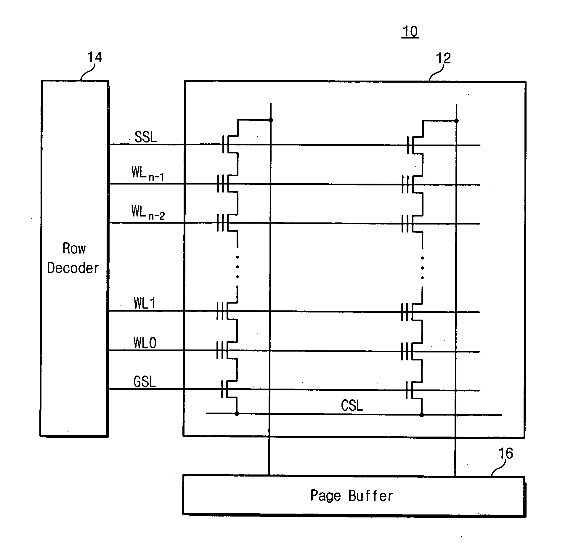
[0040]FIG. 2 is a block diagram of a flash memory device in accordance with one embodiment of the invention. Referring to FIG. 2, a flash memory device 1000 comprises a memory cell array 100 adapted to store data. Memory cell array 100 comprises a plurality of memory cells arranged in rows and columns (i.e., arranged along a plurality of word lines and a plurality of bit lines). Each of the memory cells stores 1-bit data or multi-bit data (e.g., 2-bit data). A row decoder circuit 200 is adapted to select a row of memory cell array 100, drive the selected row with a first word line voltage, and drive each of the unselected rows with a second word line voltage. For example, during a first program operation, row decoder circuit 200 drives a selected row with ...
PUM
 Abstract
Description
Claims
Application Information