Liquid crystal device, electro-optical device, projector, and micro-device

Inactive Publication Date: 2007-02-08
SEIKO EPSON CORP
View PDF29 Cites 82 Cited by
  • Summary
  • Abstract
  • Description
  • Claims
  • Application Information

AI Technical Summary

Benefits of technology

[0043] Therefore, for example, when water enters into a space between the first substrate and the second substrate from outside the micro-device, it is possible to decrease the possibility of water reach

Problems solved by technology

In general, the permeation of water inside a liquid crystal device will decrease display characteristics, thereby deteriorating the reliability of the liquid crystal device.
However, as described above, since the adhesive layer (mold member) is a member for improving the mechanical strength of a liquid crystal device, it is not sufficiently moisture-resistant to be effective in preven

Method used


Image

  • Liquid crystal device, electro-optical device, projector, and micro-device
  • Liquid crystal device, electro-optical device, projector, and micro-device
  • Liquid crystal device, electro-optical device, projector, and micro-device

Examples


Example

[0060] First Embodiment

[0061] First, an explanation will be given of a liquid crystal device of a first embodiment in this invention by referring to FIGS. 1A to 7B.

[0062] In this embodiment, an explanation will be made by referring to an active-matrix transmissive liquid crystal device in which a thin film transistor (hereinafter, abbreviated as TFT) element is used as a switching element.

[0063] Liquid Crystal Device

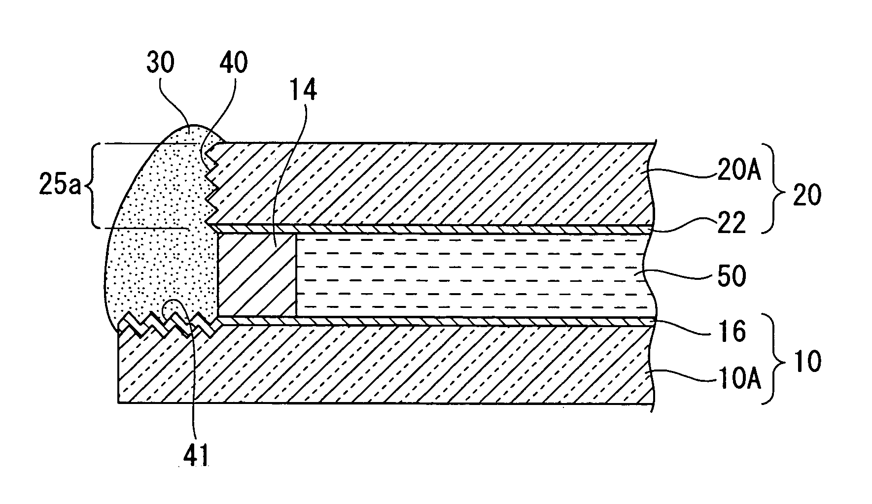
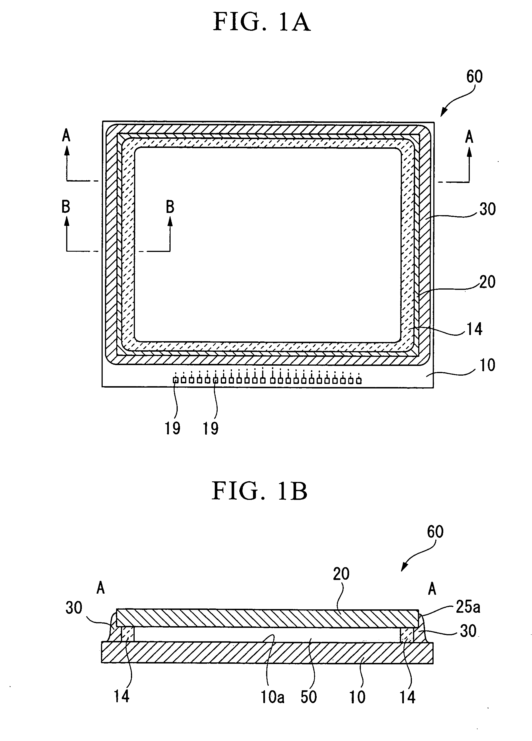
[0064]FIG. 1A is a schematic plan view that shows an active-matrix liquid crystal device of one embodiment of this invention, and FIG. 1B is a schematic cross-sectional view taken along the line A-A in FIG. 1A. Reference numeral 60 in FIGS. 1A and 1B denotes a liquid crystal device.

[0065] As shown in FIGS. 1A and 1B, the liquid crystal device 60 includes a TFT array substrate 10 (first substrate), an opposed substrate 20 (second substrate) arranged in opposition to the TFT array substrate 10, a liquid crystal layer 50 held between the TFT array substrate 10 and the ...

Example

[0277] Second Embodiment

[0278] Next, an explanation will be given of a second embodiment of the liquid crystal device in this invention by referring to FIG. 9.

[0279]FIG. 9 is a cross-sectional view that shows a liquid crystal device 160 in the 15 second embodiment.

[0280] In liquid crystal devices described in this embodiment, the same symbols are given to those of similar structure to the first embodiment for explanation, and a simplified explanation is made for a constitution similar to the first embodiment.

[0281] Furthermore, in this embodiment, the TFT array substrate 10 and the opposed 20 substrate 20 arranged so as to be mutually opposed are almost the same in dimension, when the liquid crystal device 160 is viewed from a vertical direction.

[0282] In the first embodiment, an irregular portion is formed at a mold region in the TFT array substrate 10 and the opposed substrate 20, thereby elongating an interface distance between the mold member 30 and the TFT array substrate ...


PUM


Abstract

A liquid crystal device includes: a first substrate; a second substrate opposed to the first substrate; a liquid crystal layer placed between the first substrate and the second substrate; a sealing member sealing the liquid crystal layer between the first substrate and the second substrate; a mold member provided between the first substrate and the second substrate so as to cover an outer periphery of the sealing member; and a first irregular portion formed, on at least one of the first substrate and the second substrate, over an entire region on which the mold member is arranged, wherein the mold member is provided on the first irregular portion.

Description

CROSS-REFERENCE TO RELATED APPLICATION [0001] This application claims priority from Japanese Patent Application No. 2005-227618, filed Aug. 5, 2005, and Japanese Patent Application No. 2006-139044, filed May 18, 2006, the contents of which are incorporated herein by reference. BACKGROUND [0002] 1. Technical Field [0003] The present invention relates to a liquid crystal device, an electro-optical device, a projector, and a micro-device. [0004] 2. Related Art [0005] A liquid crystal device has been used as a light modulation section for a projection display device such as a liquid crystal projector. [0006] The liquid crystal device is constituted in such a way that a sealing member is placed at a peripheral portion of a substrate between a pair of substrates, and a liquid crystal layer is sealed at the center. [0007] An electrode for applying a voltage to the liquid crystal layer is formed inside a pair of substrates, and an alignment layer for controlling the alignment of liquid crys...

Claims


Application Information

Patent Timeline
IPC IPC(8): G02F1/1339
CPCG02F1/1339
Inventor SASABAYASHI, TOMOKO
Owner SEIKO EPSON CORP
Why Eureka
Try Eureka