Test circuit and test method

a test circuit and test method technology, applied in the direction of electronic circuit testing, measurement devices, instruments, etc., can solve the problems of inability to implement testing, increasing the load on automatic test pattern generation, etc., to achieve efficient memory refresh, efficient memory refresh, and efficient memory refresh

Inactive Publication Date: 2007-02-08
RENESAS ELECTRONICS CORP
View PDF4 Cites 0 Cited by
  • Summary
  • Abstract
  • Description
  • Claims
  • Application Information

AI Technical Summary

Benefits of technology

[0017] According to an aspect of the present invention, there is provided a test method for writing and reading on a memory to be tested through a scan path flip-flop, which includes writing data to the memory from outside by inputting a write set value to the scan path flip-flop, refreshing the data written to the memory by inputting a refresh set value to the scan path flip-flop, and reading the data from the memory and outputting the data to the outside by inputting a read set value to the scan path flip-flop. This method enables implementation of memory test while refreshing the memory efficiently.
[0018] According to an aspect of the present invention, there is provided a test circuit for performing testing by shift operation of a plurality of scan paths including a memory test scan path for testing a memory, which includes a plurality of flip-flops included in each of the plurality of scan paths, wherein the number of flip-flips included in the memory test scan path is half or less than half of a largest number of flip-flips included in the scan paths. This configuration allows performing shift operation of the memory test scan path a plurality of times while performing shift operation of the scan paths different from the memory test scan path once, thereby enabling implementation of memory test while refreshing the memory efficiently.
[0019] According to an aspect of the present invention, there is provided a test circuit for performing testing by shift operation of a plurality of scan paths including a memory test scan path for testing a memory, which includes performing shift operation of the memory test scan path a plurality of times while performing shift operation of the scan paths different from the memory test scan path once, and refreshing the memory by at least one time of shift operation of the plurality of times of shift operation. This configuration enables implementation of memory test while refreshing the memory efficiently.

Problems solved by technology

The application of the above memory test technique to DRAM raises the following problems.
First problem is that, if a time period from the write setting to the read setting is longer than a data retention period or a refresh period of DRAM, it is unable to implement testing.
Another problem is an increase in load on automatic test pattern generation.
It thus increases load on the automatic test pattern generation with regard to refresh operation,
However, these patent documents only describe the method and circuit for performing write setting or read wetting on DRAM and do not describe a test method and test circuit which takes the restriction of a data retention period of DRAM into account.

Method used


Image

  • Test circuit and test method
  • Test circuit and test method
  • Test circuit and test method

Examples


first embodiment

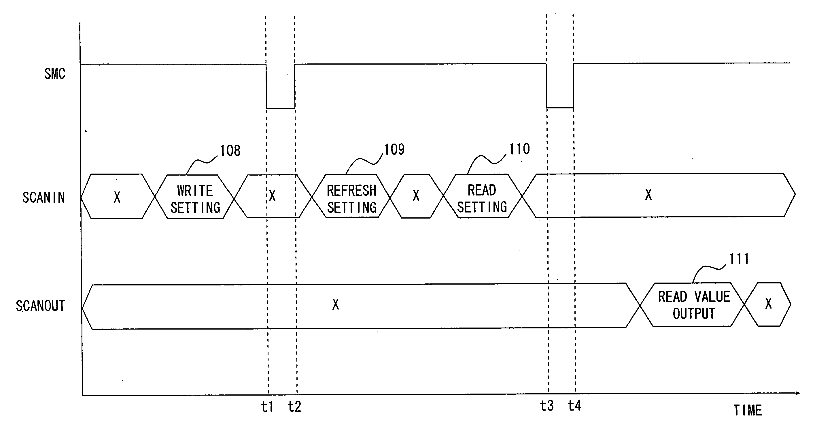
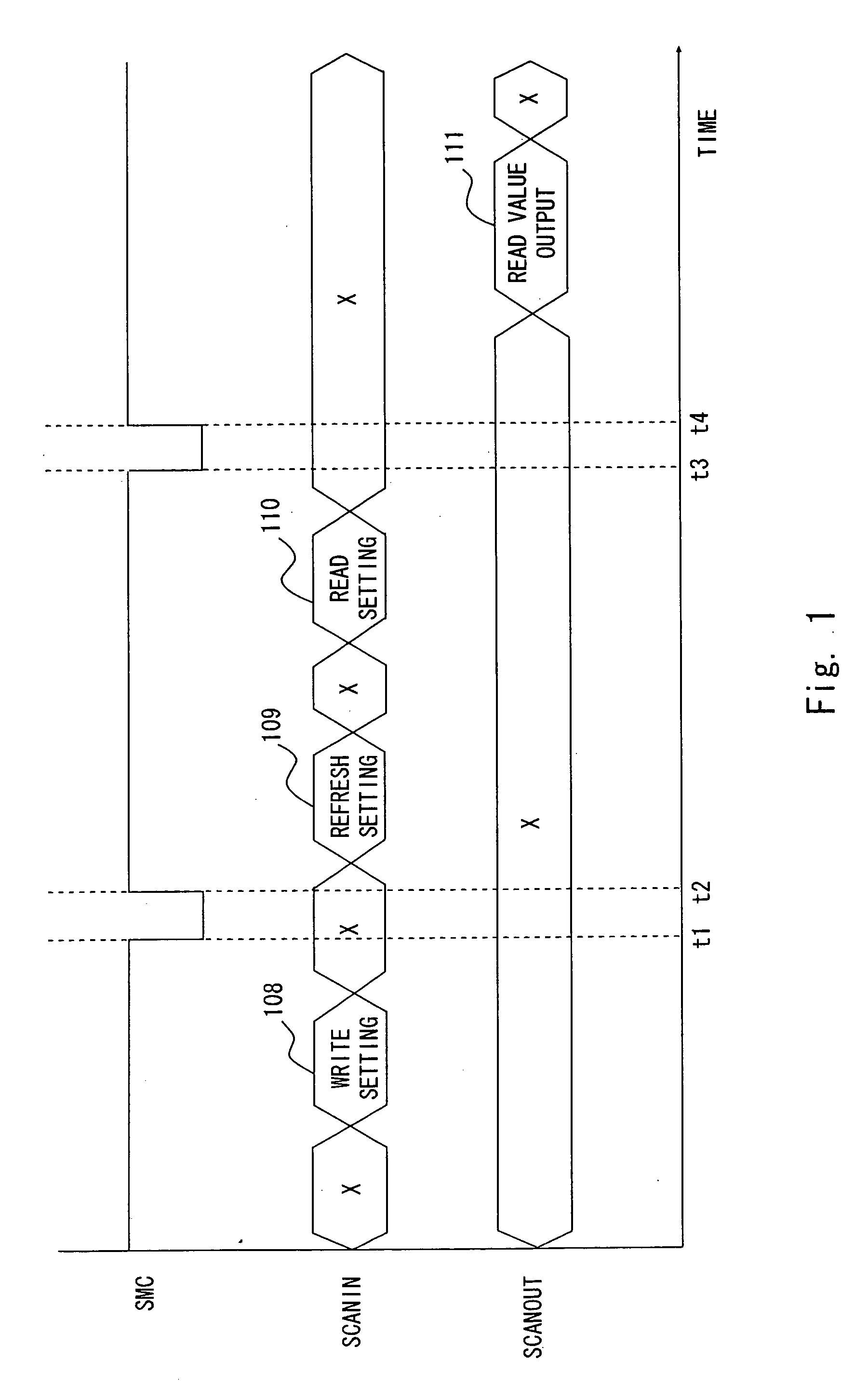
[0034] A test circuit according to an embodiment of the invention is described hereinafter with reference to FIG. 1. The test circuit according to this invention is adapted to a monolithic semiconductor device equipped with DRAM. In FIG. 1, “SMC” indicates a value of a signal SMC for selecting whether to set a scan path to shift operation or normal operation without shifting, “SCANIN” indicates a value of a scan input, and “SCANOUT” indicates a value of a scan output. In this embodiment, the value of SMC is such that “1” represents shift mode and “0” represents normal mode when no shift occurs. The state different from the shift mode is called capture mode.

[0035] Time t1 indicates when the mode changes from the shift mode to the capture mode. Time t2 indicates when the mode changes from the capture mode to the shift mode for the time firstly after t1. Time t3 indicates when the mode changes from the shift mode to the capture mode again after t2. Time t4 indicates when the mode chan...

second embodiment

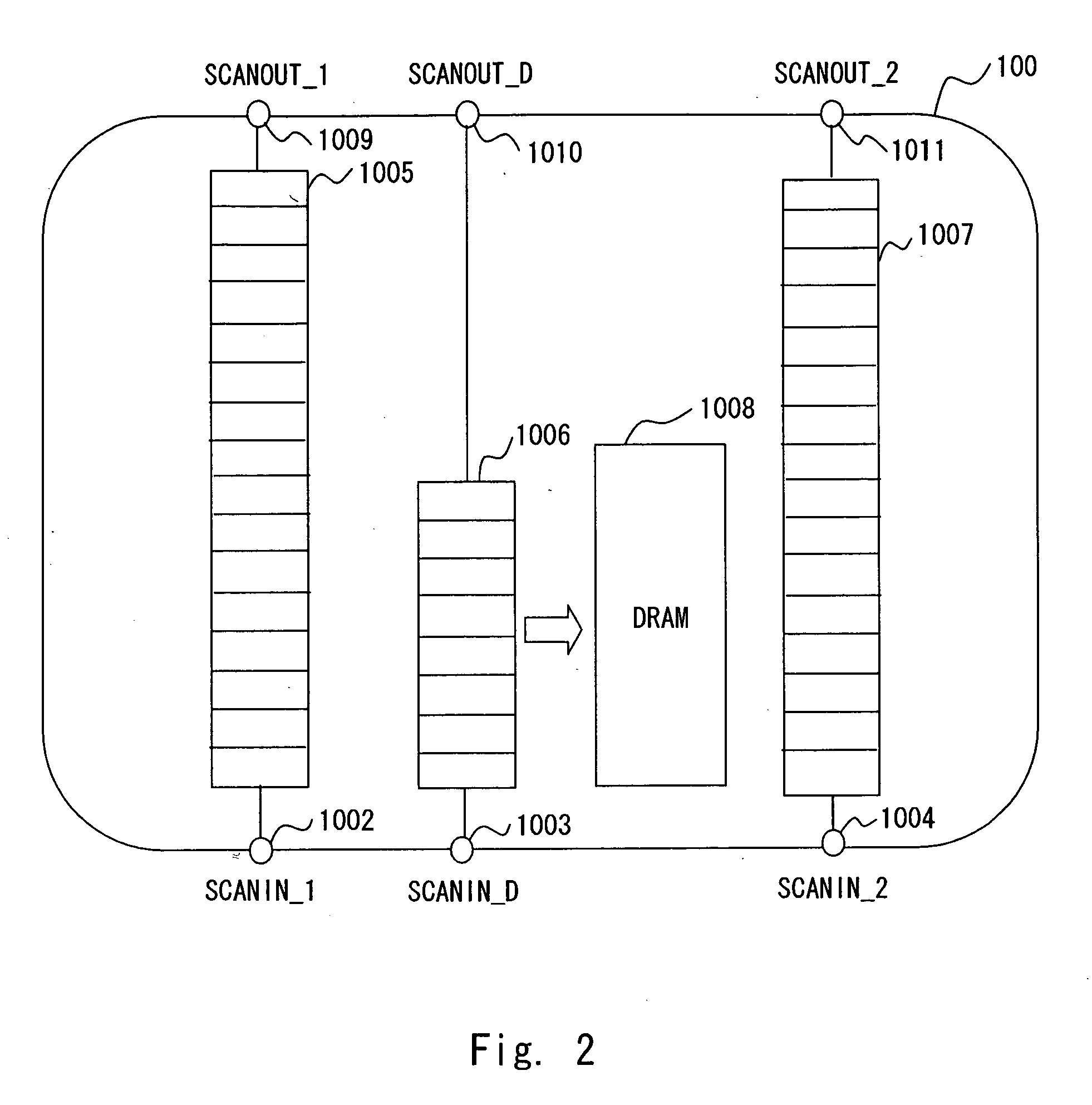
[0077] A second embodiment of the present invention is described hereinafter with reference to FIG. 2. The test circuit according to this invention is adapted to a monolithic semiconductor device equipped with DRAM. FIG. 2 shows the configuration of a test circuit according to the second embodiment of the invention. The test circuit 100 includes scan input terminals 1002, 1003 and 1004, flip-flop groups 1005, 1006 and 1007, DRAM 1008, and scan output terminals 1009, 1010 and 1011.

[0078] The test circuit 100 is composed of three scan paths. The flip-flops for setting the DRAM 1008 are included only in the scan path SCAN_D which receives a scan input through the scan input terminal 1003, outputs a scan output through the scan output terminal 1010, and has the flip-flop group 1006 to form the scan path.

[0079] The other scan paths are SCAN_1 which is composed of the scan input 1002, the flip-flop group 1005 and the scan output 1009 and SCAN_2 which is composed of the scan input 1004, ...


PUM


Abstract

A test method sets a write value to a scan flip-flop for setting a value to a memory to be tested. It then performs a series of shift operation in scan paths until setting of a read value is completed. During the shift operation, a value for refresh operation is added to the value passing through the flip-flop for setting a value to the memory to be tested.

Description

BACKGROUND OF THE INVENTION [0001] 1. Field of the Invention [0002] The present invention generally relates to test circuits and test methods, and particularly relates to a test circuit and a test method for testing an integrated circuit with a memory. [0003] 2. Description of Related Art [0004] A test technique that tests a memory or a circuit on a path passing through a memory in an integrated circuit using scan path is now widely used, as implemented into automatic test pattern generation program on a computer. However, this test technique assumes the use of static random access memory (SRAM) which does not require refreshing. It also assumes that reading is always available as long as read setting is set after writing. [0005] A conventional memory test technique using scan path is described hereinafter with reference to FIG. 12. FIG. 12 is a set waveform used in a memory test of a related art. In FIG. 12, “SMC” indicates a value of a signal SMC for selecting whether to set a sca...

Claims


Application Information

Patent Timeline
Patent Type & Authority Applications(United States)
IPC IPC(8): G01R31/28
CPCG01R31/318544G11C2029/3202G11C29/32
Inventor YAMAUCHI, HISASHI
Owner RENESAS ELECTRONICS CORP
Why Eureka
Try Eureka