Apparatus and method of predicting performance of semiconductor manufacturing process and semiconductor device, and manufacturing method of semiconductor device

a technology of semiconductor manufacturing process and semiconductor device, applied in the direction of process and machine control, semiconductor/solid-state device testing/measurement, instruments, etc., can solve the problem that the performance of a process and a device in a wafer cannot be acquired

Inactive Publication Date: 2007-02-22
KK TOSHIBA
View PDF3 Cites 10 Cited by
  • Summary
  • Abstract
  • Description
  • Claims
  • Application Information

AI Technical Summary

Benefits of technology

[0007] According to one aspect of the present invention, it is provided a performance prediction apparatus comprising: a uniform mesh data generator generating uniform mesh data by dividing a wafer surface using a uniform mesh to predict an in-plane characteristics distribution of performance with respect to each of a series of process steps; a non-uniform mesh generator generating a non-uniform mesh which non-uniformly divides the wafer surface by combining a plurality of element meshes in the uniform mesh based on the uniform mesh data and predetermined threshold values with respect to each of the series of process steps; a common mesh generator generating a common mesh by superimposing the plurality of non-uniform meshes and selecting a minimum mesh from the non-uniform meshes for every region in the wafer; a common mesh data generator generating common mesh data by representing the in-plane characteristics distribution of performance with regard to each of the series of process steps using the common mesh; and a predicting section predicting a comprehensive performance after processing the series of process steps for every region divided by the common mesh based on the plurality of the common mesh data.

Problems solved by technology

However, a mesh generation technique for an in-plane characteristics distribution simulation is not discussed, and a performance of a process and a device in a wafer cannot be acquired.

Method used


Image

  • Apparatus and method of predicting performance of semiconductor manufacturing process and semiconductor device, and manufacturing method of semiconductor device
  • Apparatus and method of predicting performance of semiconductor manufacturing process and semiconductor device, and manufacturing method of semiconductor device
  • Apparatus and method of predicting performance of semiconductor manufacturing process and semiconductor device, and manufacturing method of semiconductor device

Examples


Embodiment Construction

[0044] The embodiments of the present invention will be described with reference to the accompanying drawings. Throughout the drawings, corresponding portions are denoted by corresponding reference numerals. Each of the following embodiments is illustrated as one example, and therefore the present invention can be variously modified and implemented without departing from the spirits of the present invention.

[0045] Various aspects of the present invention provide apparatus and method of predicting performance in a wafer of a semiconductor manufacturing process and a semiconductor device, which are capable of reducing a calculation amount and calculation time when predicting the performance in the wafer by an in-plane characteristics distribution simulation, and a manufacturing method of a semiconductor device.

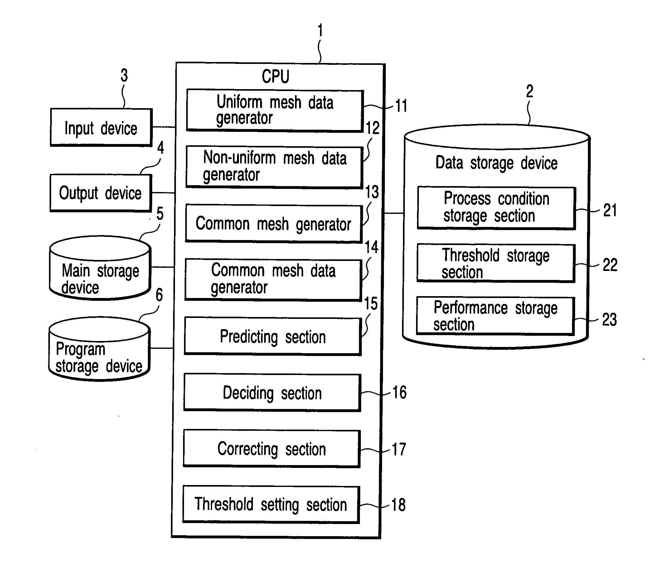
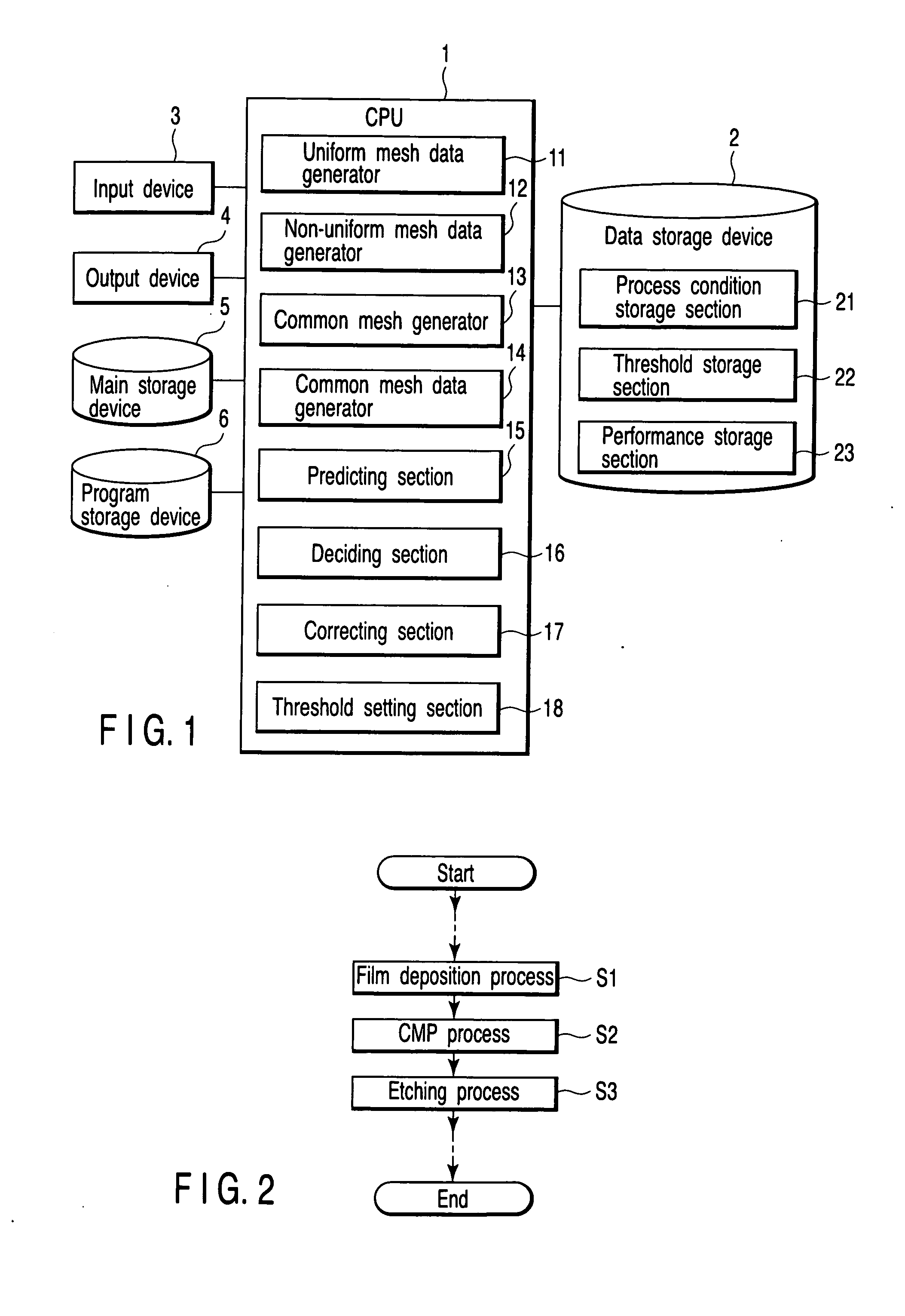
[0046]FIG. 1 shows an example of a performance prediction apparatus (a simulation apparatus) according to an embodiment of the present invention. As shown in FIG. 1, the perfo...


PUM


Abstract

Apparatus and method of predicting performance of a semiconductor manufacturing process and device, which reduces simulation resources to predict the performance distribution in the wafer and manufacturing method of a semiconductor device are disclosed. According to one aspect, it is provided a performance prediction apparatus comprising a uniform mesh data generator generating uniform mesh data by dividing a wafer using a uniform mesh to predict an in-plane characteristics distribution of performance in a series of process steps, a non-uniform mesh generator generating a non-uniform mesh by combining element meshes based on the uniform mesh data and predetermined threshold, a common mesh generator generating a common mesh by superimposing the non-uniform meshes and selecting a minimum mesh by region, a common mesh data generator generating common mesh data by representing the performance using the common mesh, and a predicting section predicting a comprehensive performance after processing the series of processes.

Description

CROSS-REFERENCE TO RELATED APPLICATIONS [0001] This application is based upon and claims the benefit of priority from prior Japanese Patent Application No. 2005-235970, filed Aug. 16, 2005, the entire contents of which are incorporated herein by reference. BACKGROUND OF THE INVENTION [0002] 1. Field of the Invention [0003] The present invention relates to a characteristics distribution simulation technique in a wafer, and more particularly to apparatus and method of predicting performance in a wafer of a semiconductor manufacturing process and a semiconductor device by using an in-plane characteristics distribution simulation, and a manufacturing method of a semiconductor device. [0004] 2. Description of the Related Art In a semiconductor manufacturing process, an in-plane characteristics distribution simulation which predicts a performance of process and device in an entire wafer is carried out. In a current semiconductor manufacturing process, a performance and / or yield of process...

Claims


Application Information

Patent Timeline
Patent Type & Authority Applications(United States)
IPC IPC(8): H01L21/66
CPCG05B17/02
Inventor KAWABATA, KENJI
Owner KK TOSHIBA
Why Eureka
Try Eureka