Backside ground type flip chip semiconductor package

a flip chip and semiconductor technology, applied in semiconductor devices, semiconductor/solid-state device details, electrical apparatus, etc., can solve the problems of limited enhancement of thermal properties of the package product, disadvantageously deteriorating electrical properties of the product, and chip with sensitive properties and high available frequency, etc., to achieve the effect of improving heat releasing properties

Inactive Publication Date: 2007-03-01
SAMSUNG ELECTRO MECHANICS CO LTD
View PDF2 Cites 47 Cited by
  • Summary
  • Abstract
  • Description
  • Claims
  • Application Information

AI Technical Summary

Benefits of technology

[0018] The present invention has been made to solve the foregoing problems of the prior art and therefore an object according to certain embodiments of the present invention is to provide a backside ground flip chip semiconductor package which releases heat generated from a chip through a backside ground to improve heat releasing properties.

Problems solved by technology

However, the path fails to enable heat generated from the chip 10 to be entirely released to the outside, thereby limitedly enhancing thermal properties of the package product.
This increases parasitic capacitance, thereby disadvantageously deteriorating electrical properties of the product.
As a result, the chip which exhibits sensitive properties and a high available frequency, and processes a high-power signal maybe jeopardized by heat releasing problems, radio wave radiation and radio wave noises.

Method used


Image

  • Backside ground type flip chip semiconductor package
  • Backside ground type flip chip semiconductor package
  • Backside ground type flip chip semiconductor package

Examples


first embodiment

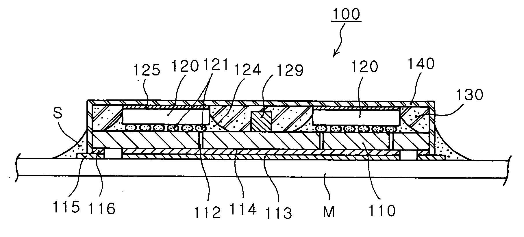
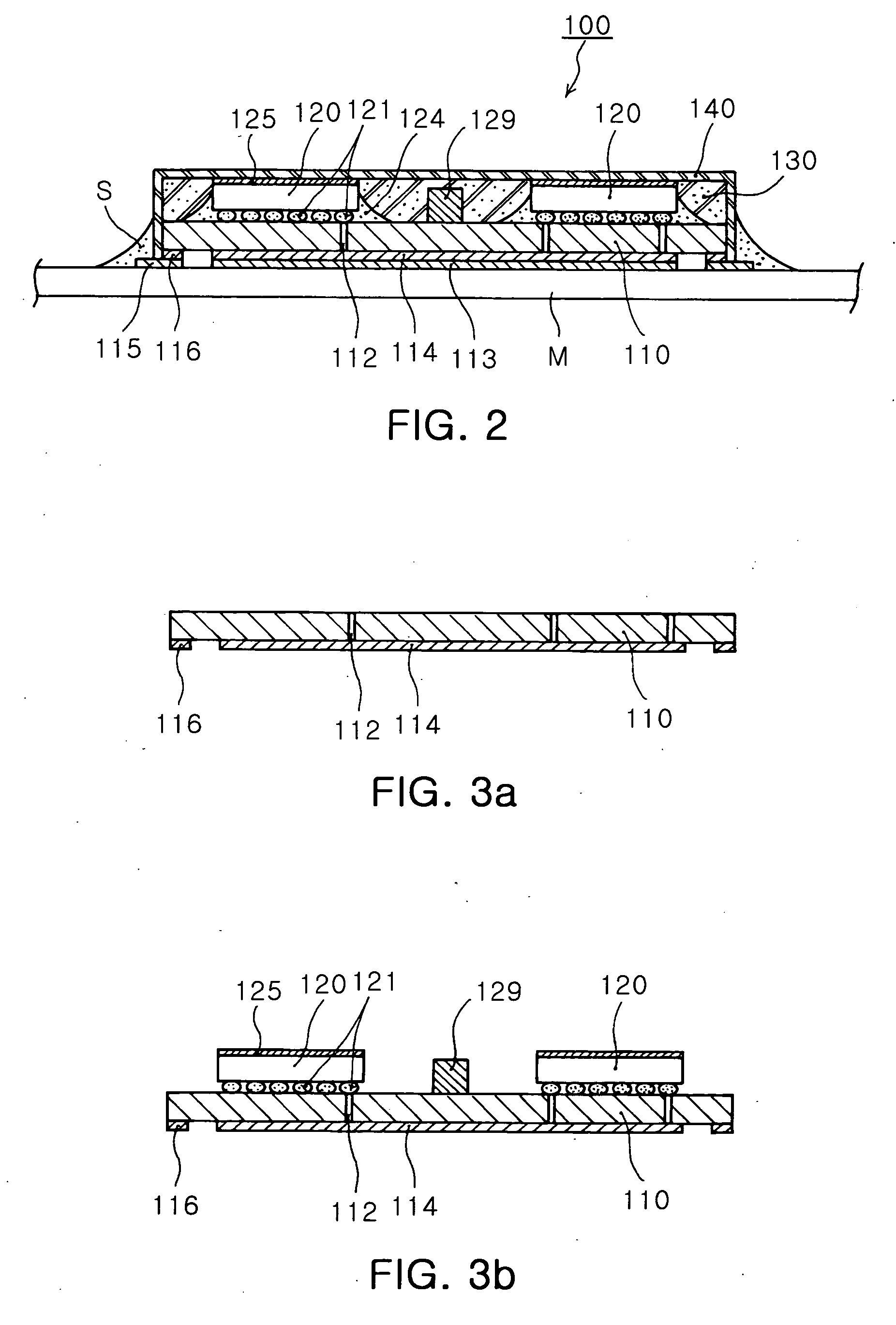
[0046]FIG. 2 is a cross-sectional view illustrating a backside ground flip chip semiconductor package. The flip chip semiconductor package of the invention, as shown in FIG. 2, has a heat releasing path connected to a main substrate via a backside ground electrode and a ground path connected to the main substrate. The flip chip semiconductor package includes a substrate 110, a chip 120, an encapsulant or molded part 130 and a conductive metal layer 140.

[0047] The substrate 110 has various circuits pattern-printed thereon and at least one chip 120 and a passive device 129 mounted thereover to suit the circuits.

[0048] The substrate 110 has at least one heat-releasing via structure 112 connected to a metal connecting pad 114 provided on an underside of the substrate 110. At least one lower ground pad 116 is disposed in the vicinity of the metal connecting pad 114.

[0049] The chip 120 has a plurality of ball pads (not illustrated) arrayed on an underside surface thereof at a predetermi...

second embodiment

[0073]FIG. 4 is a cross-sectional view illustrating a backside ground flip chip semiconductor package according to the invention. The package 100a of the invention, as shown in FIG. 4, includes a substrate 110, a chip 120, a molded part 130 and a conductive metal layer 140. Therefore, the same components were given the same reference signs and will not be explained further.

[0074] The substrate 110 has a heat-releasing via structure 112 and a ground via structure 112a formed therein. The heat-releasing via structure 112 has an upper end connected to bump balls 121 on which the chip 120 is flip-bonded. The ground via structure 112a has an upper end connected to an upper ground pad 118 formed on the substrate 110.

[0075] The heat-releasing via structure 112 and the ground via structure 112a each has a lower end connected to a metal connecting pad 114a provided on an underside of the substrate 110. The metal connecting pad 114a is electrically connected to an electrode of the main subst...

third embodiment

[0085]FIG. 6 is a cross-sectional view illustrating a backside ground flip chip semiconductor according to the invention. The package 100b of the invention includes a substrate 110, a chip 120, a molded part 130 and a metal conductive layer 140. The same components were given the same reference signs and will not be explained further.

[0086] In a case where the molded part 130 is formed higher than a backside ground electrode 125 of the chip, the molded part 130 has an opening 135 for exposing the backside ground electrode 125 to the outside, corresponding to the backside ground electrode 125. The opening 135 is smaller than the backside ground electrode 125.

[0087] Accordingly, such a molded part 130 has a greater height than a molded part formed upto the backside ground electrode 125 and then polished, thereby leading to a bigger size of the product. However, the molded part 130 structured as just described further ensures the chip to be protected from external environment, thereby...


PUM


Abstract

In a flip chip semiconductor package, a substrate is provided. At least one chip is flip-bonded onto the substrate to electrically connect to a circuit pattern-printed on the substrate. A molded part is formed on the substrate so as to expose a backside ground of the chip. Also, a conductive metal layer is extended along an outer surface of the molded part to electrically connect to the backside ground. According to the invention, heat generated from the chip is released through the backside ground to improve heat releasing properties. Furthermore, the electrical ground is formed without creating a parasitic component to enhance electrical properties.

Description

CLAIM OF PRIORITY [0001] This application claims the benefit of Korean Patent Application No. 2005-80310 filed on Aug. 30, 2005 in the Korean Intellectual Property Office, the disclosure of which is incorporated herein by reference. BACKGROUND OF THE INVENTION [0002] 1. Field of the Invention [0003] The present invention relates to a flip chip semiconductor package having a backside ground and more particularly, a backside flip chip semiconductor package which releases heat generated from a chip through a backside ground to improve heat releasing properties and has the electrical ground formed free from a parasitic component to enhance electrical properties. [0004] 2. Description of the Related Art [0005] With recent advancement in personal mobile telecommunications, a great number of devices or parts have been highly dense and multi-functional, especially buoyed by development of softwares and techniques of IC integration. Most strikingly, not only each part or block but also an ov...

Claims


Application Information

Patent Timeline
Patent Type & Authority Applications(United States)
IPC IPC(8): H01L23/34
CPCH01L23/3121H01L23/3677H01L2224/73253H01L2224/16145H01L2224/73204H01L2224/32225H01L24/48H01L2924/3025H01L2924/30107H01L2924/19105H01L2924/16152H01L2924/15311H01L2924/01079H01L2924/01078H01L2924/01046H01L2224/73265H01L2224/48227H01L2224/16225H01L25/16H01L23/552H01L23/49816H01L23/482H01L23/49805H01L2924/00H01L2924/00012H01L2224/451H01L2924/00014H01L24/45H01L24/73H01L2924/00015H01L2224/05599H01L23/34H01L23/52
Inventor JEONG, IN HOKIM, NAM HEUNG
Owner SAMSUNG ELECTRO MECHANICS CO LTD
Why Eureka
Try Eureka