Package for mounting semiconductor device

a semiconductor device and package technology, applied in the direction of solid-state devices, basic electric elements, metal-patterned materials, etc., can solve the problems of low thermal emissivity and deterioration of heat release properties (heat-dissipating properties) of lsi, and achieve the effect of improving heat release properties (heat-dissipating properties) of an lsi

Inactive Publication Date: 2005-12-13
LONGITUDE LICENSING LTD
View PDF23 Cites 0 Cited by
  • Summary
  • Abstract
  • Description
  • Claims
  • Application Information

AI Technical Summary

Benefits of technology

[0011]It is therefore an object of the present invention to provide a package for mounting a semiconductor device which is capable of improving heat release properties (heat-dissipating properties) of an LSI.

Problems solved by technology

Therefore, its thermal emissivity is low.
This causes the deterioration of heat release properties (heat-dissipating properties) of the LSI.

Method used


Image

  • Package for mounting semiconductor device
  • Package for mounting semiconductor device
  • Package for mounting semiconductor device

Examples


first embodiment

[0028](First Embodiment)

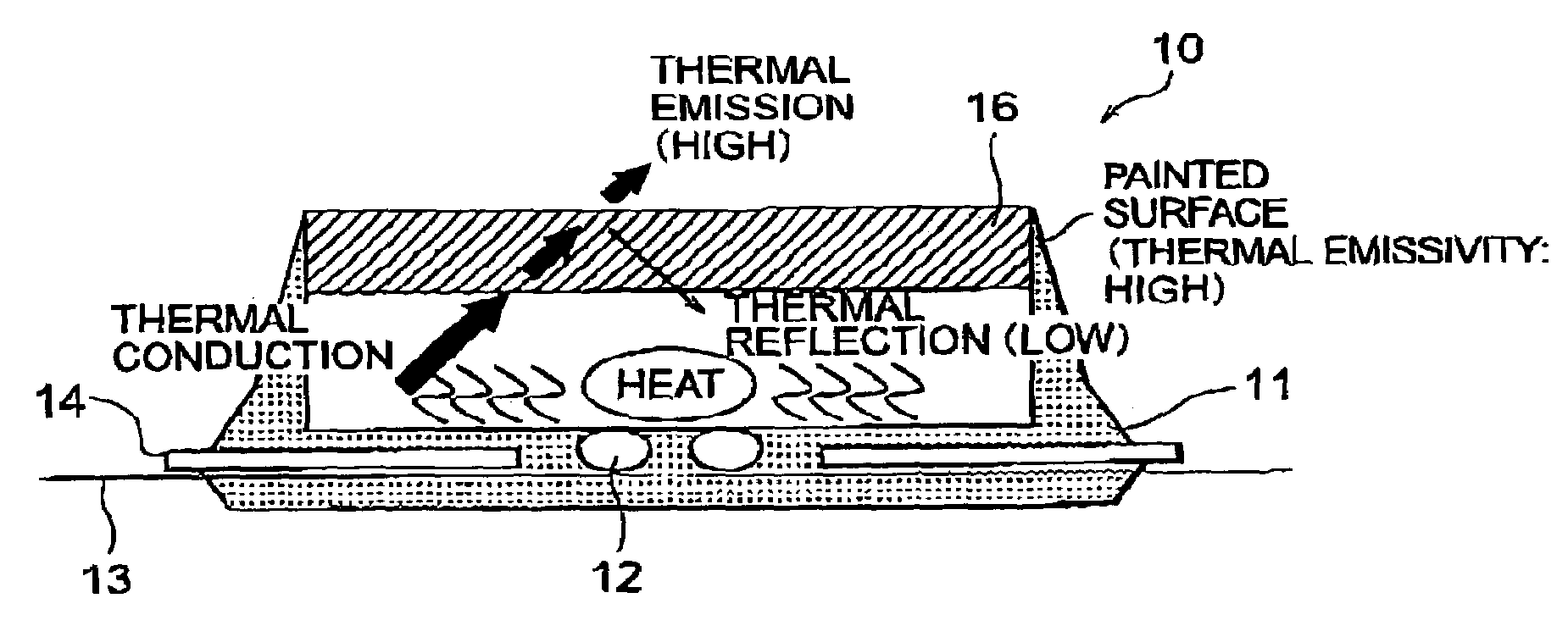
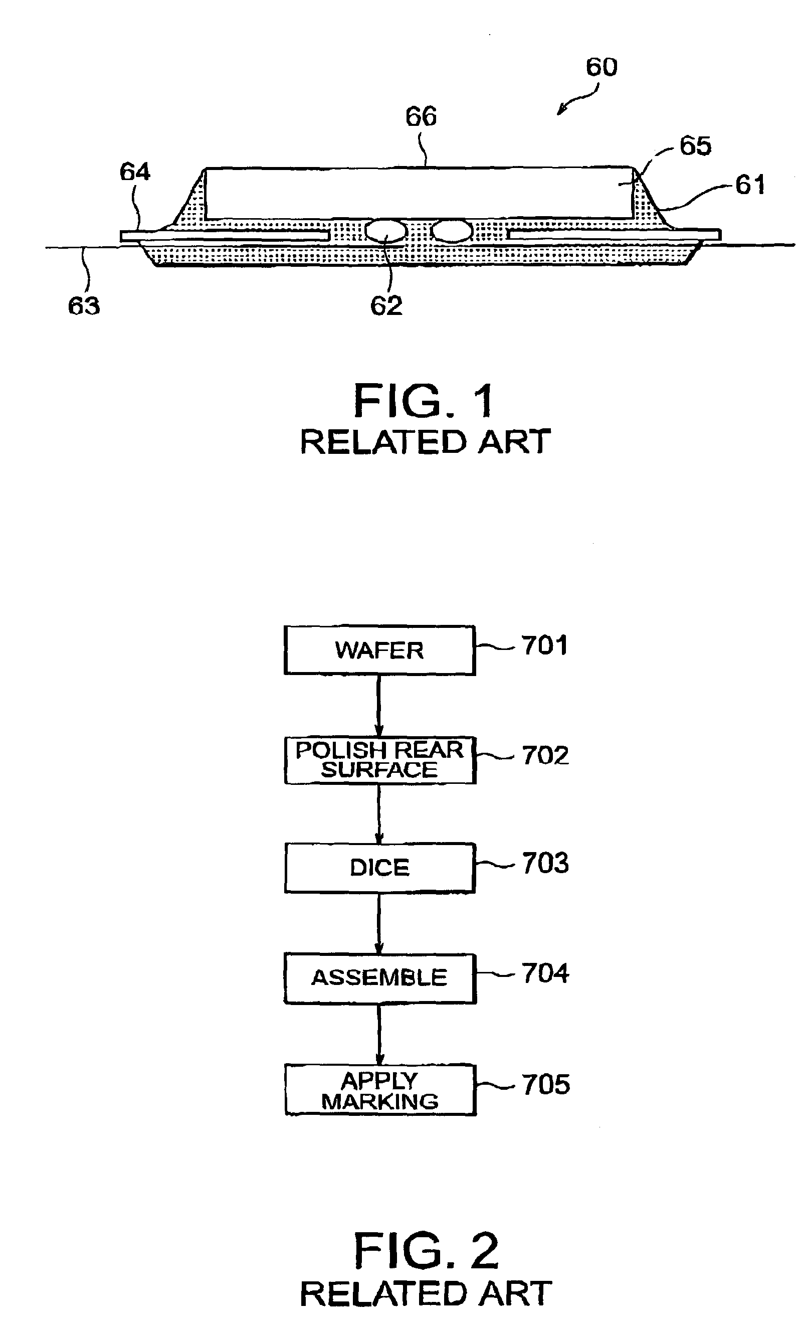
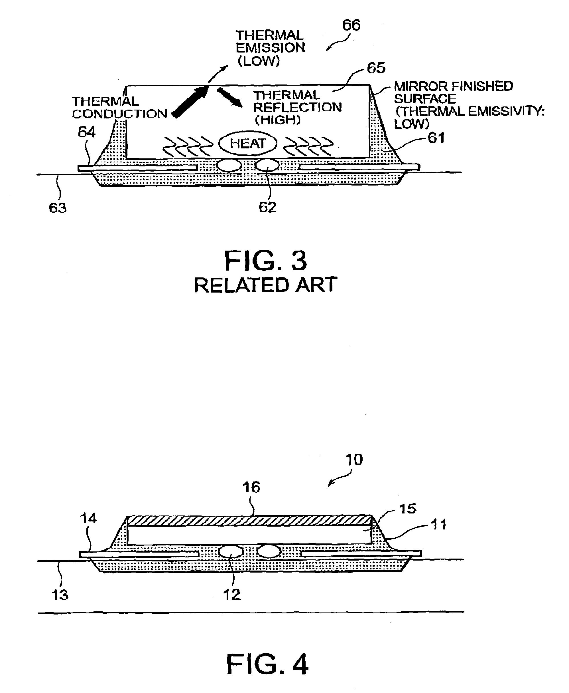
[0029]Referring to FIG. 4, description will be made of a package for mounting a semiconductor device according to the present invention, taking an example of a tape carrier package (TCP). Herein, it is to be noted that the package according to the present invention is not limited to the tape carrier package (TCP), and is applicable to other various packages such as a chip size package (CSP).

[0030]In FIG. 4, a tape carrier package 10 has a resin 11, press-bonded portions 12, a lead 13 and a tape 14, and an LSI 15 is mounted on this tape carrier package 10. With such a structure, a mirror-finished exposed surface of the LSI 15 is covered with a covering material 16.

[0031]For the tape carrier package (TCP) 10 in which the material having a low thermal emissivity to an atmosphere is exposed, the entire exposed surface of the LSI 15 is covered with a material having high thermal emissivity, for example, a paint, a tape or a seal having a thermal emissivity of 0.8 ...

second embodiment

[0046](Second Embodiment)

[0047]Referring to FIGS. 7 and 8, description will be made of a package for mounting a semiconductor device according to a second embodiment of the present invention, taking an example of the tape carrier package (TCP).

[0048]In the second embodiment, a part of the exposed surface of the LSI 15, which is mirror-finished, is covered with the covering material 16, and it is different in this point from the package for mounting the semiconductor device in the first embodiment (FIG. 4). The constitution of other parts is the same as that of the package for mounting the semiconductor device shown in FIG. 4 and will not be described.

[0049]Specifically, a paint or the like is applied in a manner to outline a mark portion 17 such as a product name (characters or symbols). In this method, while a part where the thermal emissivity is low remains, application to the mark portion 17 and application of a paint can be performed together, thus providing a merit of preventin...


PUM


Abstract

A package for mounting a semiconductor device has a surface exposed to an atmosphere. The exposed surface is covered with a covering material such as a paint, a tape or a seal.

Description

[0001]This application claims priority to prior application JP2002-107452, the disclosure of which is incorporated herein by reference.BACKGROUND OF THE INVENTION[0002]The present invention relates to a package for mounting a semiconductor device having an exposed surface, in particular relates to a package for mounting a semiconductor device suitable for a tape carrier package (TCP) or a chip size package (CSP).[0003]Referring to FIG. 1, description will be made of a related tape carrier package (TCP).[0004]In FIG. 1, a tape carrier package 60 has a resin 61, press-bonded portions 62, a lead 63 and a tape 64, and an LSI 65 is mounted on this tape carrier package 60.[0005]Subsequently, an assembling method of the tape carrier package 60 will be described with reference to FIG. 2.[0006]First, a wafer is provided (step 701), and a rear (back) surface of the wafer is polished (step 702).[0007]Next, the polished wafer is diced (step 703), and is then assembled (step 704). Finally, desir...

Claims


Application Information

Patent Timeline
Patent Type & Authority Patents(United States)
IPC IPC(8): H01L23/31H01L23/29H01L23/34H01L23/373
CPCH01L23/3135H01L23/3164H01L23/3737H01L2924/0002H01L2924/00H01L23/36
Inventor MOURI, MORIHIKOOKUMA, SADAYUKITAKAHASHI, YASUSHIONO, TAKAOSAKAGUCHI, YOSIHIRONAKAMURA, ATSUSHIMIYAZAWA, TOSHIO
Owner LONGITUDE LICENSING LTD
Why Eureka
Try Eureka