Semiconductor device and method of manufacturing the same

a semiconductor and semiconductor technology, applied in the field of semiconductor devices, can solve the problems of lowering the freedom of wiring layout over the mounting substrate, and achieve the effect of improving the heat-release properties of semiconductor devices and improving the reliability of semiconductor devices

Inactive Publication Date: 2011-06-09
RENESAS ELECTRONICS CORP
View PDF3 Cites 18 Cited by
  • Summary
  • Abstract
  • Description
  • Claims
  • Application Information

AI Technical Summary

Benefits of technology

[0016]The following explains briefly the effect acquired by the typical invention among the inventions disclosed in the present application.
[0017]The typical embodiments can improve the heat-release properties of semiconductor device.
[0018]Furthermore, the typical embodiments can improve the reliability of semiconductor device.

Problems solved by technology

In the case of that type of semiconductor device, however, there is required, also at the side of the mounting substrate, placing a bump land (electrode pad) coupled with the heat-releasing external terminal directly thereon, which lowers the freedom of wiring layout over the mounting substrate.

Method used


Image

  • Semiconductor device and method of manufacturing the same
  • Semiconductor device and method of manufacturing the same
  • Semiconductor device and method of manufacturing the same

Examples


embodiment 1

[0111]The semiconductor device and the method of manufacturing thereof (manufacturing process) according to an embodiment of the present invention are described below referring to the drawings.

[0112]

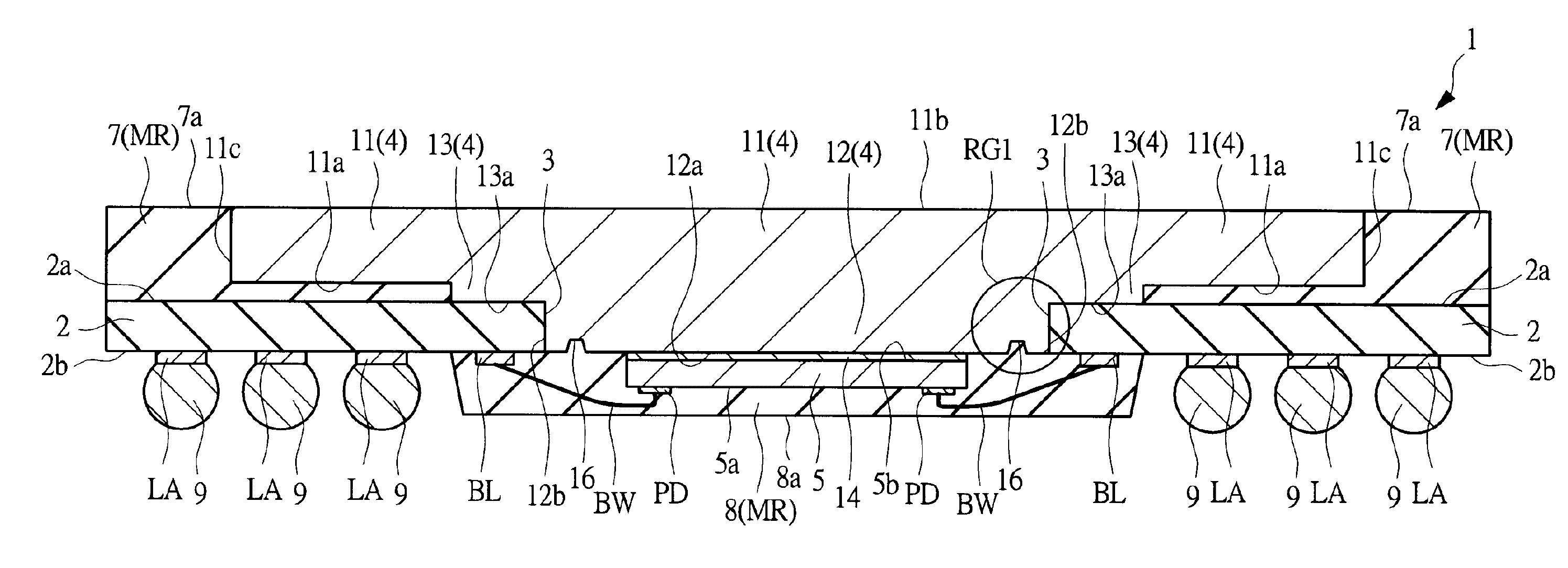
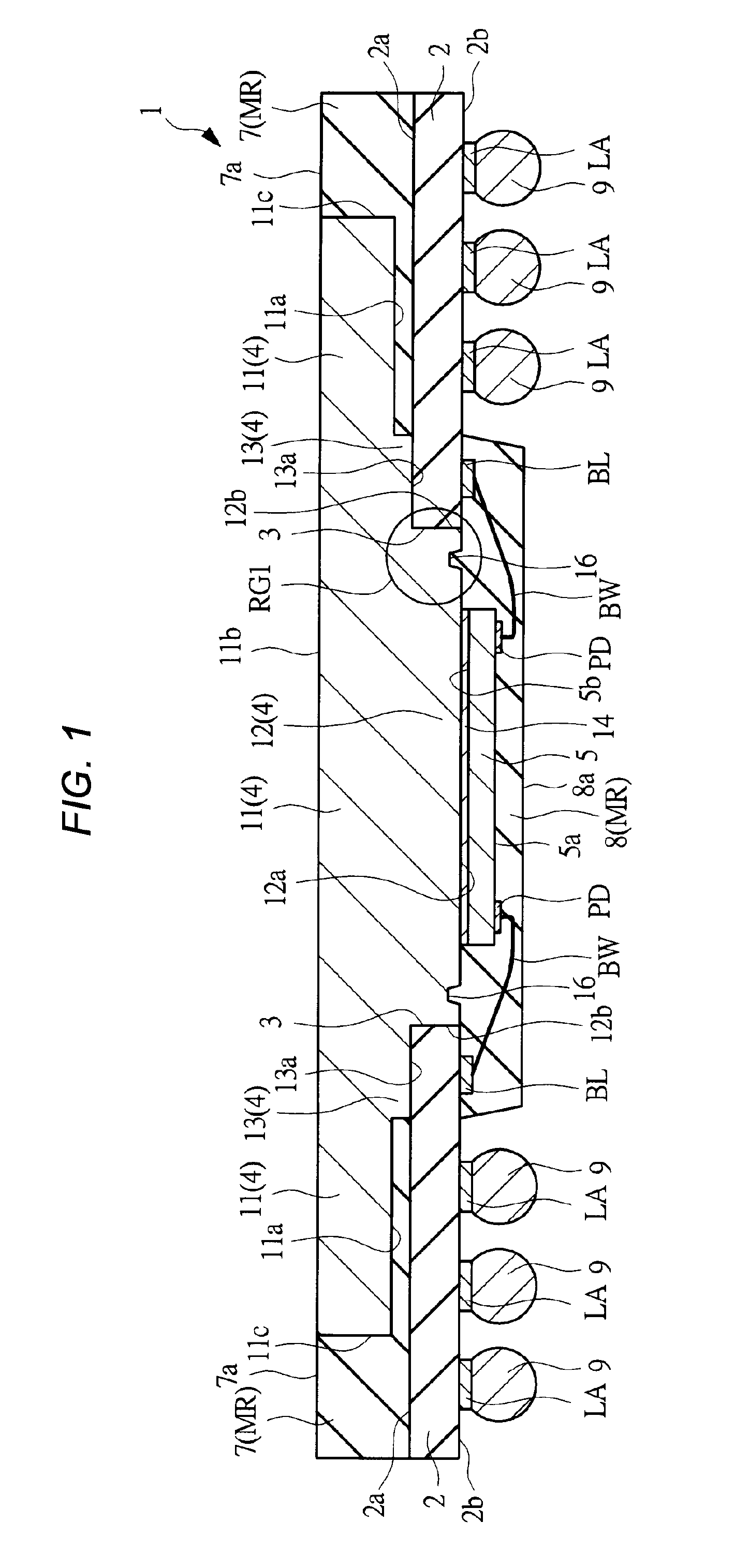
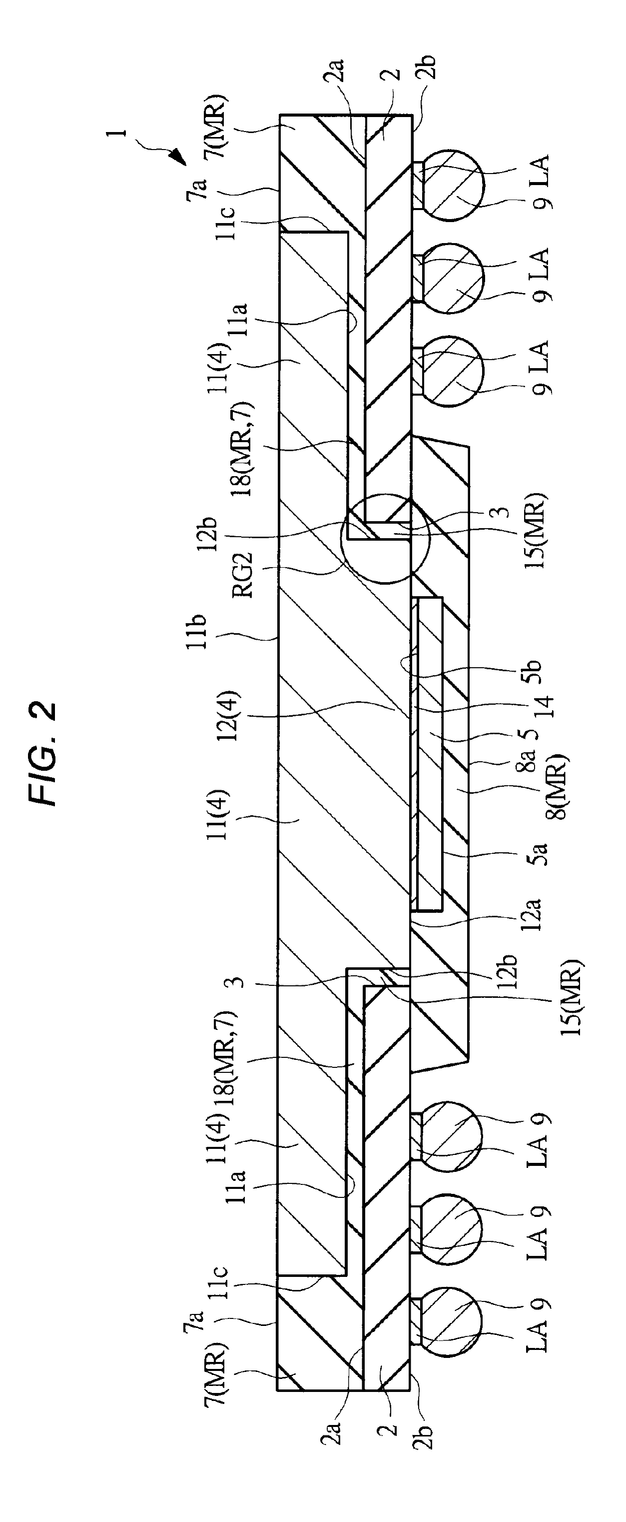
[0113]FIG. 1 and FIG. 2 show cross-sectional views (side surface cross-sectional views) of a semiconductor device 1 according to an embodiment of the present invention. FIG. 3 and FIG. 4 show main-part cross-sectional views (part-enlarged cross sectional views) of the semiconductor device 1. FIG. 5 is an upper surface view (plan view) of the semiconductor device 1. FIG. 6 is a lower surface view (bottom face view, rear surface view, plan view) of the semiconductor device 1. FIG. 7 is a plane perspective view (upper surface view) of the semiconductor device 1, illustrating the upper surface side of the semiconductor device 1 when seen through a sealing portion 7. FIG. 8 is a plane perspective view (lower surface view) of the semiconductor device 1, illustrating the lower side view of the ...

embodiment 2

[0266]According to the manufacturing process described in the embodiment 1, the semiconductor chip 5 is mounted over the convex part 12 of the heat-releasing plate 4, and then the heat-releasing plate 4 with the mounted semiconductor chip 5 is placed in the through-hole 3 of the wiring substrate 31. According to the embodiment 2, however, the heat-releasing plate 4 is placed in the through-hole 3 of the wiring substrate 31 before mounting the semiconductor chip 5 over the convex part 12 of the heat-releasing plate 4, and then the semiconductor chip 5 is mounted over the convex part 12 of the heat-releasing plate 4, positioned in the through-hole 3. The case will be described below referring to FIGS. 68 to 74.

[0267]FIG. 68 illustrates the flow diagram of another manufacturing process of semiconductor device 1 according to the embodiment 2, which flow diagram corresponds to that of FIG. 22 of the embodiment 1. FIGS. 69 to 74 are plan views and cross-sectional views during the manufact...

embodiment 3

[0279]FIG. 75 and FIG. 76 are cross-sectional views (side surface cross-sectional views) of a semiconductor device 1a of the embodiment 3, corresponding to FIG. 1 and FIG. 2 of the embodiment 1, respectively.

[0280]According to the semiconductor device 1 of the embodiment 1, the main surface 12a of the convex part 12 of the heat-releasing plate 4 is in almost the same plane as that of the lower surface 2b of the wiring substrate 2, and the height of the main surface 12a of the convex part 12 of the heat-releasing plate 4 is almost the same as the height of the lower surface 2b of the wiring substrate 2.

[0281]In contrast, according to the semiconductor device 1a of the embodiment 3, the main surface 12a of the convex part 12 of the heat-releasing plate 4 is not in the same plane as that of the lower surface 2b of the wiring substrate 2, positioned (height position) between the lower surface 2b and the upper surface 2a of the wiring substrate 2. That is, according to the semiconductor ...


PUM


Abstract

The heat-release properties of semiconductor device are to be improved and the reliability thereof is to be improved.
The semiconductor device has a wiring substrate, a heat-releasing plate having a convex part inserted into a through-hole of the wiring substrate, a semiconductor chip mounted over the convex part of the heat-releasing plate, and a bonding wire coupling an electrode pad of the semiconductor chip with a bonding lead of the wiring substrate, and further has a sealing portion covering a portion of an upper surface of the wiring substrate, a sealing portion covering a portion of a lower surface of the wiring substrate including the semiconductor chip and the bonding wire, and a solder ball placed over a lower surface of the wiring substrate. In manufacturing the semiconductor device, the heat-releasing plate is positioned at the upper surface side of the wiring substrate such that the convex part is positioned in the through-hole, and a groove in the main surface of the convex part is forcibly widened to swage the convex part and to be fixed to the wiring substrate.

Description

CROSS-REFERENCE TO RELATED APPLICATION[0001]The disclosure of Japanese Patent Application No. 2009-278214 filed on Dec. 8, 2009 including the specification, drawings and abstract is incorporated herein by reference in its entirety.BACKGROUND OF THE INVENTION[0002]The present invention relates to a semiconductor device and a method of manufacturing thereof, and in particular, to a technology effective for a highly heat-releasing semiconductor package and a method of manufacturing thereof.[0003]A BGA package type semiconductor device is manufactured by mounting a semiconductor chip over a wiring substrate, by coupling electrically an electrode of the semiconductor chip with a coupling terminal of the wiring substrate through the use of a bonding wire, by sealing the semiconductor chip and the bonding wire with a resin, and then by connecting a solder ball with the rear surface of the wiring substrate.[0004]Japanese Patent Laid-Open No. 1999-163230 (Patent Document 1) describes the tec...

Claims


Application Information

Patent Timeline
Patent Type & Authority Applications(United States)
IPC IPC(8): H01L23/34H01L21/60
CPCH01L21/561H01L2924/30107H01L23/13H01L23/3128H01L23/367H01L23/3675H01L24/48H01L24/49H01L24/83H01L24/85H01L24/97H01L2224/32245H01L2224/45144H01L2224/48091H01L2224/48227H01L2224/49171H01L2224/73265H01L2224/83192H01L2224/92247H01L2224/97H01L2924/01029H01L2924/01033H01L2924/01046H01L2924/01047H01L2924/01057H01L2924/01078H01L2924/01079H01L2924/01082H01L2924/15311H01L2924/1532H01L2924/15321H01L21/565H01L2924/01014H01L2224/85H01L2924/014H01L2924/01075H01L2924/01006H01L2924/01005H01L2924/00014H01L2224/83H01L2924/00H01L2924/3512H01L2924/00012H01L24/45H01L24/73H01L2224/05554H01L2924/14H01L2924/181H01L2224/45015H01L2924/207
Inventor TAKAHASHI, NORIYUKI
Owner RENESAS ELECTRONICS CORP
Why Eureka
Try Eureka