

Method of depositing Ge-Sb-Te thin film
- Summary
- Abstract
- Description
- Claims
- Application Information
AI Technical Summary
Benefits of technology
Problems solved by technology
Method used
Image

Examples
first embodiment
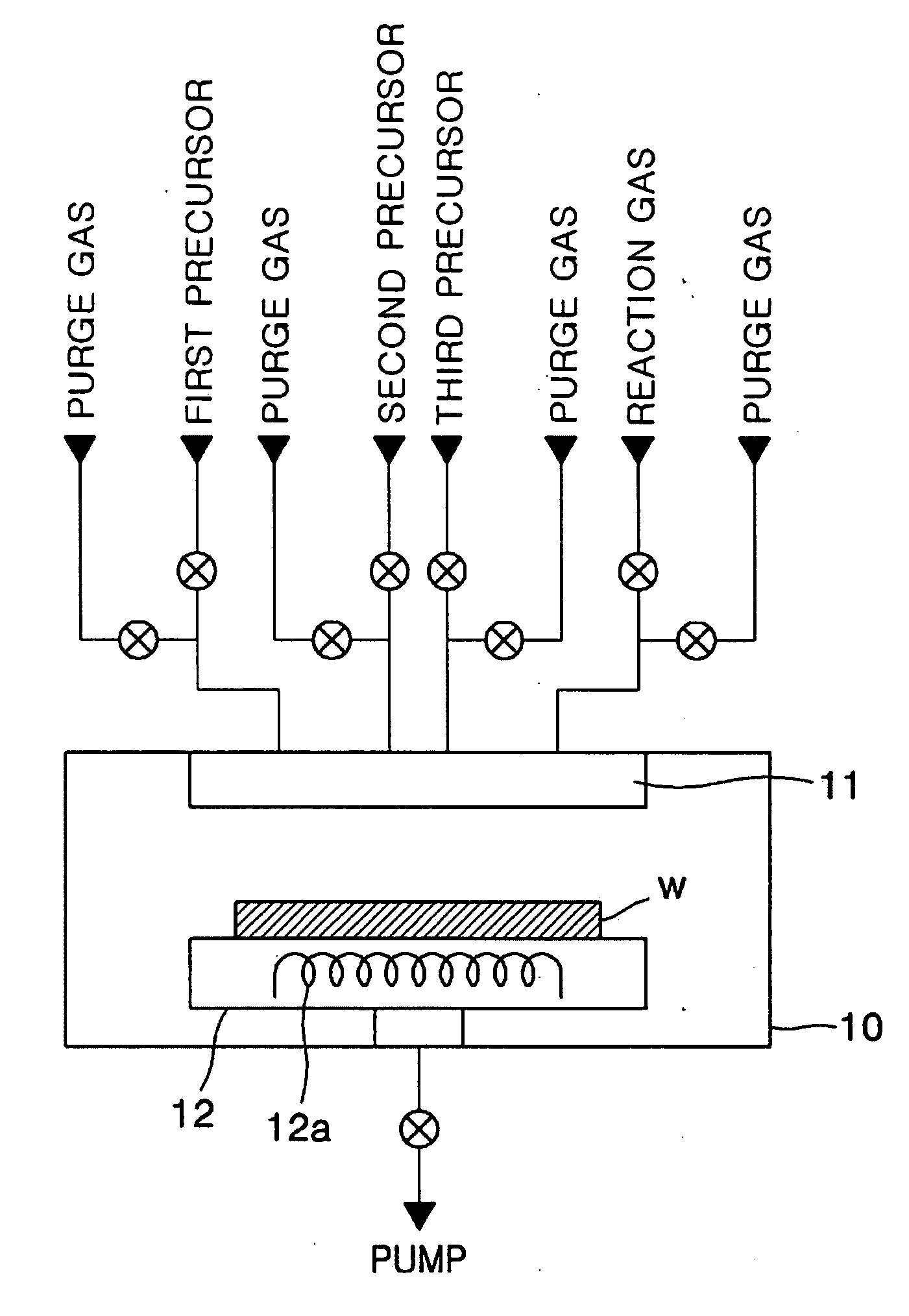
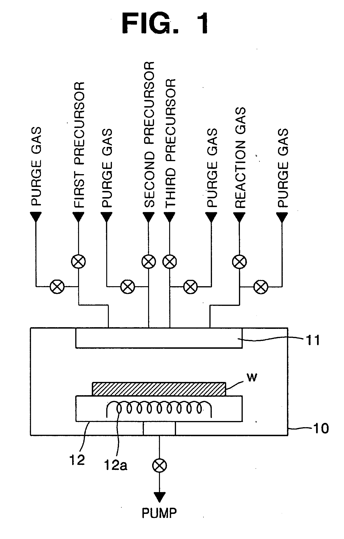
[0041] First, FIG. 3 is a view showing the flow of a method of depositing a Ge—Sb—Te thin film according to a first embodiment of the present invention.
[0042] Referring to FIG. 3, the method of depositing the Ge—Sb—Te thin film according to the first embodiment of the present invention includes a Ge—Sb—Te thin-film forming step S20 of feeding and purging the first precursor including any one of Ge, Sb and Te, the second precursor including another one of Ge, Sb and Te and the third precursor including the other one of Ge, Sb and Te into and from the chamber 10 in which the wafer w is mounted to deposit the Ge—Sb—Te thin film on the wafer w, a reaction gas feeding step S10 of feeding the reaction gas into the chamber 10 while the first to third precursors are fed and purged, and a step of adjusting the thickness of the film formed by repeating the Ge—Sb—Te thin-film forming step S20.
[0043] First, in the reaction gas feeding step S10, at least one selected from the group consisting ...
second embodiment
[0050]FIG. 4 is a view showing the flow of a method of depositing a Ge—Sb—Te thin film according to a second embodiment of the present invention.
[0051] Referring to FIG. 4, the method of depositing the Ge—Sb—Te thin film according to the second embodiment of the present invention includes a Ge—Sb—Te thin-film forming step S120 of feeding and purging the first precursor including any one of Ge, Sb and Te, the second precursor including another one of Ge, Sb and Te and the third precursor including the other one of Ge, Sb and Te into and from the chamber 10 in which the wafer w is mounted to deposit the Ge—Sb—Te thin film on the wafer w, a reaction gas feeding step S10 of feeding the reaction gas into the chamber 10 while the first to third precursors are fed and purged, and a step of adjusting the thickness of the film formed by repeating the Ge—Sb—Te thin-film forming step S120.
[0052] As shown in FIG. 4, the Ge—Sb—Te thin-film forming step S120 is performed by sequentially perform...
third embodiment
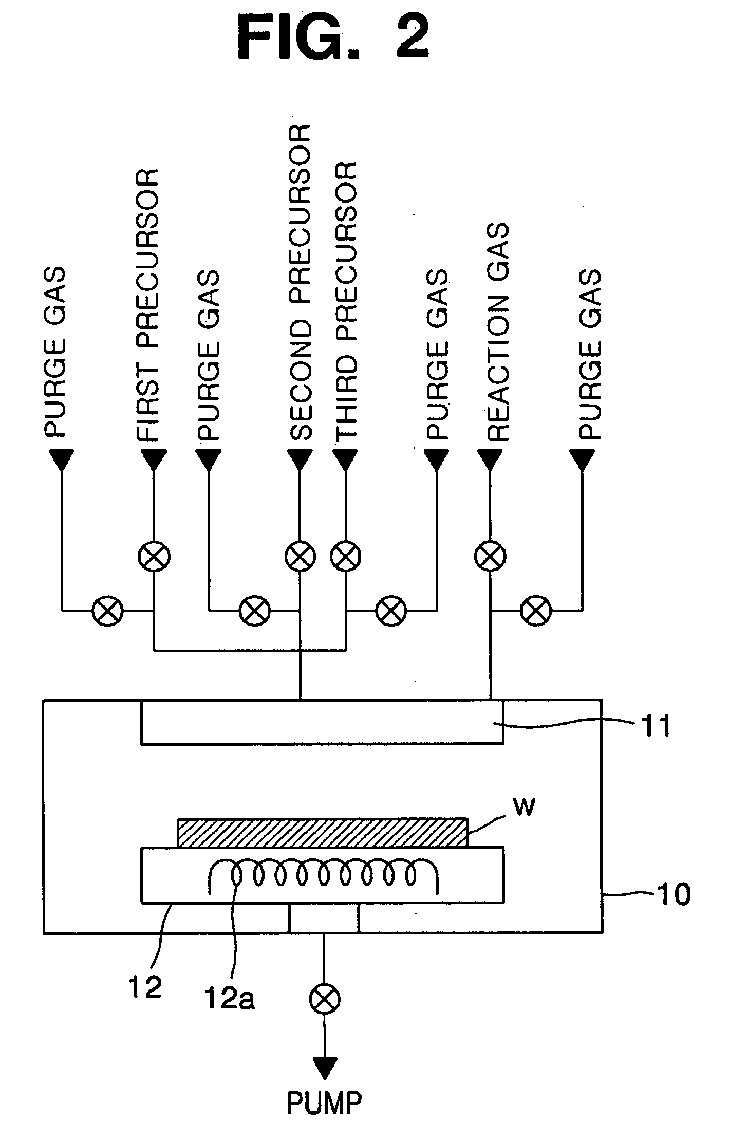
[0055]FIG. 5 is a view showing the flow of a method of depositing a Ge—Sb—Te thin film according to a third embodiment of the present invention.
[0056] Referring to FIG. 5, the method of depositing the Ge—Sb—Te thin film according to the third embodiment of the present invention includes a Ge—Sb—Te thin-film forming step S220 of feeding and purging the first precursor including any one of Ge, Sb and Te, the second precursor including another one of Ge, Sb and Te and the third precursor including the other one of Ge, Sb and Te into and from the chamber 10 in which the wafer w is mounted to deposit the Ge—Sb—Te thin film on the wafer w, a reaction gas feeding step S10 of feeding the reaction gas into the chamber 10 while the first to third precursors are fed and purged, and a step of adjusting the thickness of the film formed by repeating the Ge—Sb—Te thin-film forming step S220.
[0057] As shown in FIG. 5, the Ge—Sb—Te thin-film forming step S220 is performed by sequentially performin...
PUM
| Property | Measurement | Unit |
|---|---|---|
| Temperature | aaaaa | aaaaa |
| Temperature | aaaaa | aaaaa |
| Pressure | aaaaa | aaaaa |
Abstract
Description
Claims
Application Information