Diffractive, polarization modulating optical devices

a technology of polarization modulation and optical devices, applied in the field of optical devices, can solve the problems of compromising integrity and less suitable for volume low cost manufacturing, and achieve the effect of little or no diffractive

Inactive Publication Date: 2007-03-08
DE TECH
View PDF14 Cites 32 Cited by
  • Summary
  • Abstract
  • Description
  • Claims
  • Application Information

AI Technical Summary

Benefits of technology

[0055] It will be appreciated that this allows optical devices to be produced with various adjacent domains. Each domain may provide both a diffractive effect and a phase modulation or retardation effect, or it may provide just a phase modulation or retardation effect only. In the latter instance the local micro-relief structure will be such as to provide little or no diffractive effect. In other instances, depending on the polarization of the illumination light, it may be possible to provide domains in which the polarization modulation effect, whilst present, is not apparent, due to the appropriate orientation of the plane of polarization of the illumination light with the optical axis of the anisotropic second layer.
[0056] Thus, the encoding surface may be designed so that over most if not all of its operating area it serves both to produce a diffractive image and also to produce a polarization encoded image. However, numerous hybrid arrangements are possible. Thus the encoding surface may have at different locations thereon a region which generates a diffraction image and separately therefrom a region which produces a polarization encoded image. These systems share the common adva

Problems solved by technology

In the main, even though these type A security features have become more easily recognisable and accepted by the general public, there have been cases where they have been counterfeited thus compromising their integrity.
The origination, mastering an

Method used


Image

  • Diffractive, polarization modulating optical devices
  • Diffractive, polarization modulating optical devices
  • Diffractive, polarization modulating optical devices

Examples


first embodiment

[0088] Referring to FIG. 4, in this embodiment, the whole area of the device acts both to apply a diffractive effect (type A) to produce a first image and a phase modulation / retardation (type B) to produce a second image.

[0089] In this case the relief structure (p, D) is similar to that described in that of the previously described grating design for a Type A diffractive security optical device. In this embodiment the polymerisable liquid crystal material is RMM34 (from Merck) but other similar types are available. This material has extraordinary and ordinary refractive indices ne=1.68 and no=1.525, giving Δn=0.155.

[0090] The optical retardation δ is given by δ=2d (ne−no), the factor 2 being because the device is used in reflective mode. d is the thickness of the optically anisotropic layer.

[0091] For λ=0.5 μm for average visible light, this gives:

d=0.8065 μm for (½λ plate)

d=0.4032 μm for (¼λ plate)

[0092] It is known that a ½λ retardation alters the direction of polarization o...

second embodiment

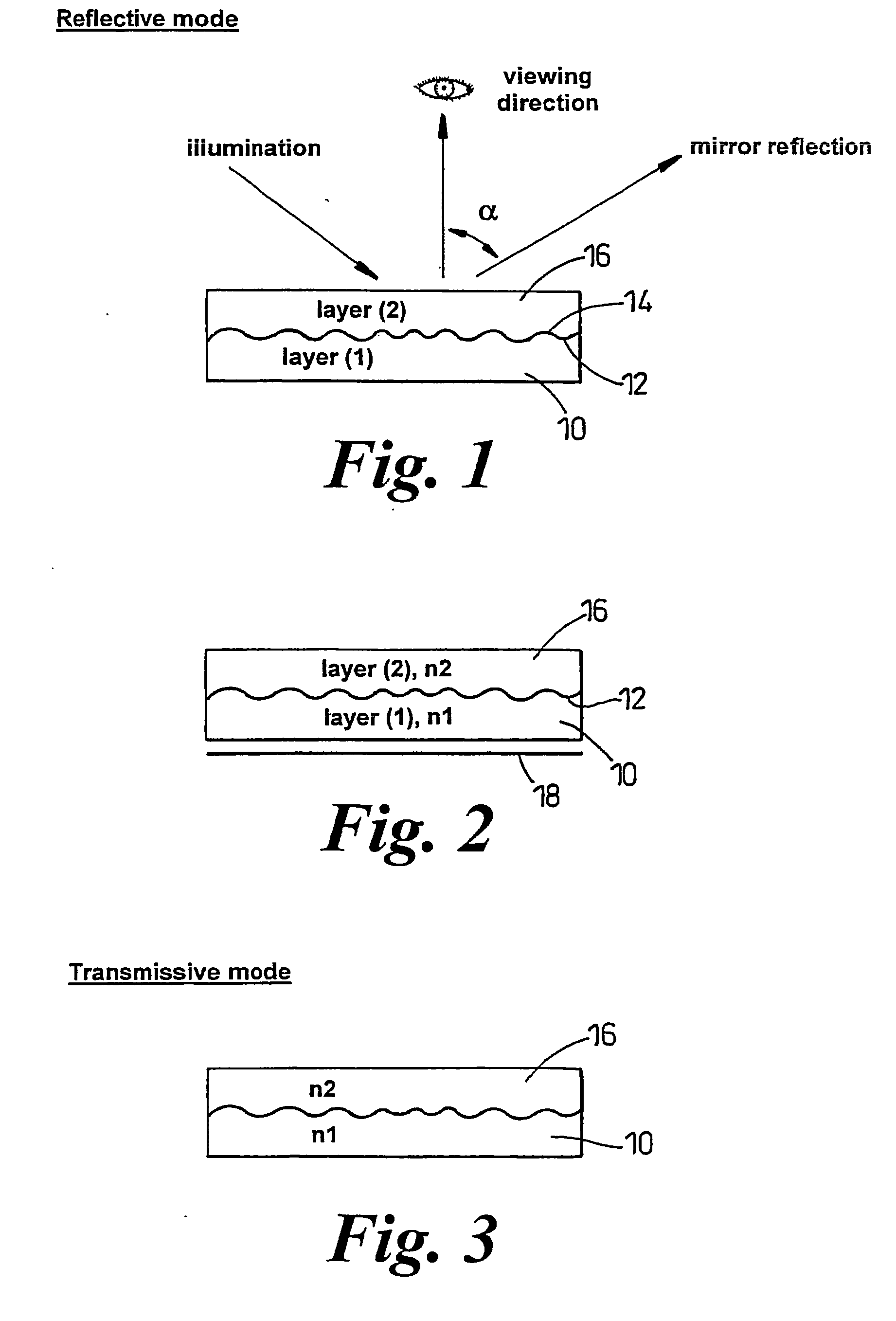
[0098] In this embodiment illustrated in FIG. 6, the device is constructed to be viewed in transmission mode. The layer 20 is isotropic but transparent and carries a micro-relief diffractive structure 22 which serves also to align the anisotropic liquid crystal material layer 26.

[0099] In this case the retardation is given by δ=(ne−no).d, and so for ½λ requires d=1.613 μm (λ=0.5 μm).

[0100] In a variation of embodiment, the interface may be only partly coated with a reflective layer, with the remainder being transmissive so that the device operates as ½λ plate in transmission and a full λ plate in reflection (e.g. no retardation). Accordingly, in this variation a thickness d=0.8065 μm may be selected to give operation of ¼λ in transmissive mode and operation of ½λ in reflective mode.

third embodiment

[0101] In this embodiment, all or part of the optical device is constructed so that, although the substrate carries a micro-relief grating structure, its diffractive properties are minimal or negligible. Referring to Equation (1) it will be seen that if p (pitch of the grating) is small (e.g. p=0.2 or 0.1 μm or less) then all the diffractive orders are suppressed. Furthermore, if the depth of the structure is very small, e.g. D˜0.05 μm or less, then it is known from diffraction theory that the diffraction efficiency of the grating will be very low, in fact very little light is diffracted. However with these parameters (e.g. p˜0.1 μm, D˜0.05 μm) it should be emphasised that alignment will continue to occur quite efficiently, and this regime may be termed “alignment only”. In this regime the grating parameters for p or D are as above. In practice the device will diffract poorly if either of the parameters is in this regime and certainly does so if both are of the same regime.

[0102] T...


PUM


Abstract

An optical device includes an encoding surface having a micro-relief pattern (22) over at least part thereof designed to produce a predetermined diffracted first image when illuminated in use, and an optically anisotropic layer (26) such as a polymerized liquid crystal provided whereby at least part of the micro-relief pattern (22) induces local orientation of the optically anisotropic layer (26) thereby to impose a predetermined polarization modulation, thereby to produce a predetermined polarization dependent second image when illuminated in use.

Description

[0001] The present invention relates to optical devices, to methods for fabricating such devices, and to articles incorporating such devices. The invention also extends to methods of authenticating articles, documents etc. using such devices, and to optical data storage. [0002] In one aspect the invention relates to optical devices primarily used to provide optical security for valuable documents and identification products such as ID cards, passports, visas, currency, security threads and branded goods. However, in other aspects such devices may be adapted for other purposes. [0003] There are, broadly speaking, a number of families of known optical security devices. One important type of these is known under the acronym DOVID (Diffractive Optically Variable Image Device), otherwise referred to herein as type A devices. In these devices images and / or information are encoded in the form of diffractive micro-optical structures. A large variety of different features based on diffractiv...

Claims


Application Information

Patent Timeline
IPC IPC(8): G03H1/00G02B5/18G02B5/30G03H1/02G06K19/16
CPCG02B5/1861G02B5/3016G03H1/0011G03H1/0244G03H1/0256G03H1/0272G07D7/0013G03H2001/187G03H2001/2276G03H2240/54G03H2240/55G03H2250/38G03H2270/52G03H2001/0016B42D25/324B42D25/328B42D25/351B42D25/364B42D25/373G03H2001/184G03H2001/188G07D7/0032
Inventor EZRA, DAVID
Owner DE TECH
Why Eureka
Try Eureka