Eureka AIR delivers breakthrough ideas for toughest innovation challenges, trusted by R&D personnel around the world.

Image sensor chip package fabrication method

Active Publication Date: 2007-03-15
POLIGHT TECH LTD
View PDF4 Cites 1 Cited by
  • Summary
  • Abstract
  • Description
  • Claims
  • Application Information

AI Technical Summary

Benefits of technology

[0012] mounting a transparent cover to the carrier, the adhesive means adhering to the cover and configured in a manner so as to define a sealing space for a photosensitive area of the image sensor chip therein, and the base and the cover allowing one end of the conductive pieces to be exposed out therefrom.

Problems solved by technology

As a result, a larger space is needed in order for the chip package to operate properly.
This method of connecting wires 156 is complex and as a result it is also expensive.
The dust-particles obscure the optical path and produce errors in the image sensing process.
Moreover, the bonding wires 156, exposed in the space 150, lack protection and may thus easily be damaged by dust-particles entering the space 150.

Method used


Image

  • Image sensor chip package fabrication method
  • Image sensor chip package fabrication method
  • Image sensor chip package fabrication method

Examples


Embodiment Construction

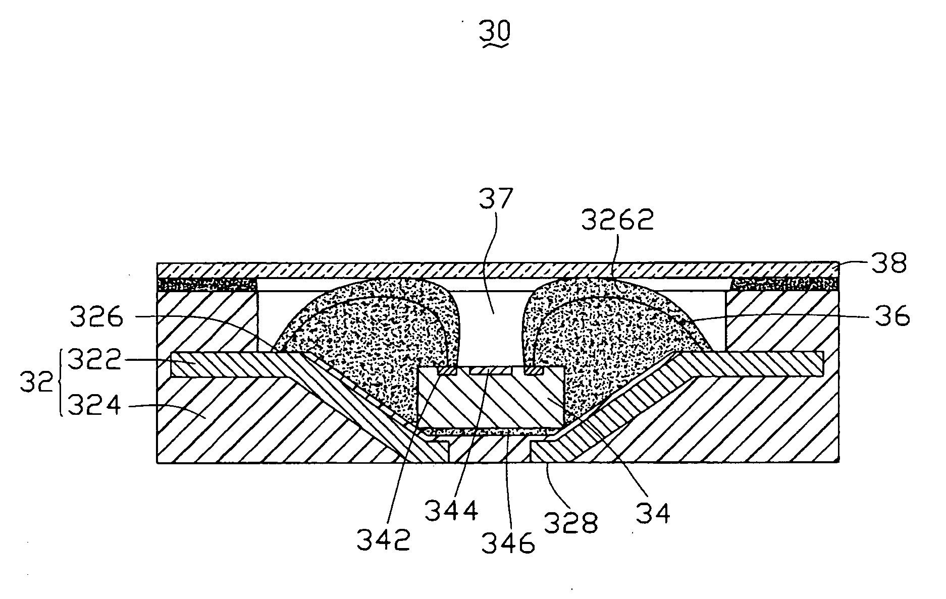
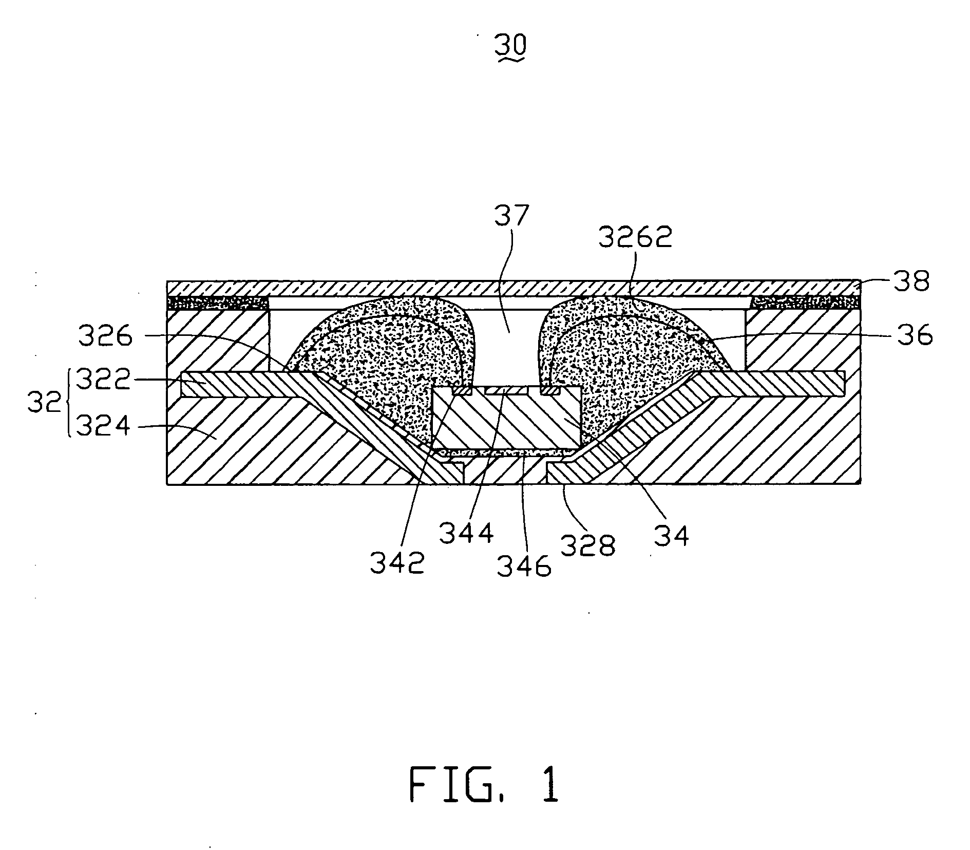
[0024] Referring to FIG. 1, an image sensor chip package 30 in accordance with a preferred embodiment is shown. The image sensor chip package 30 includes a carrier 32, a chip 34, a number of bonding wires 36 and a cover 38.

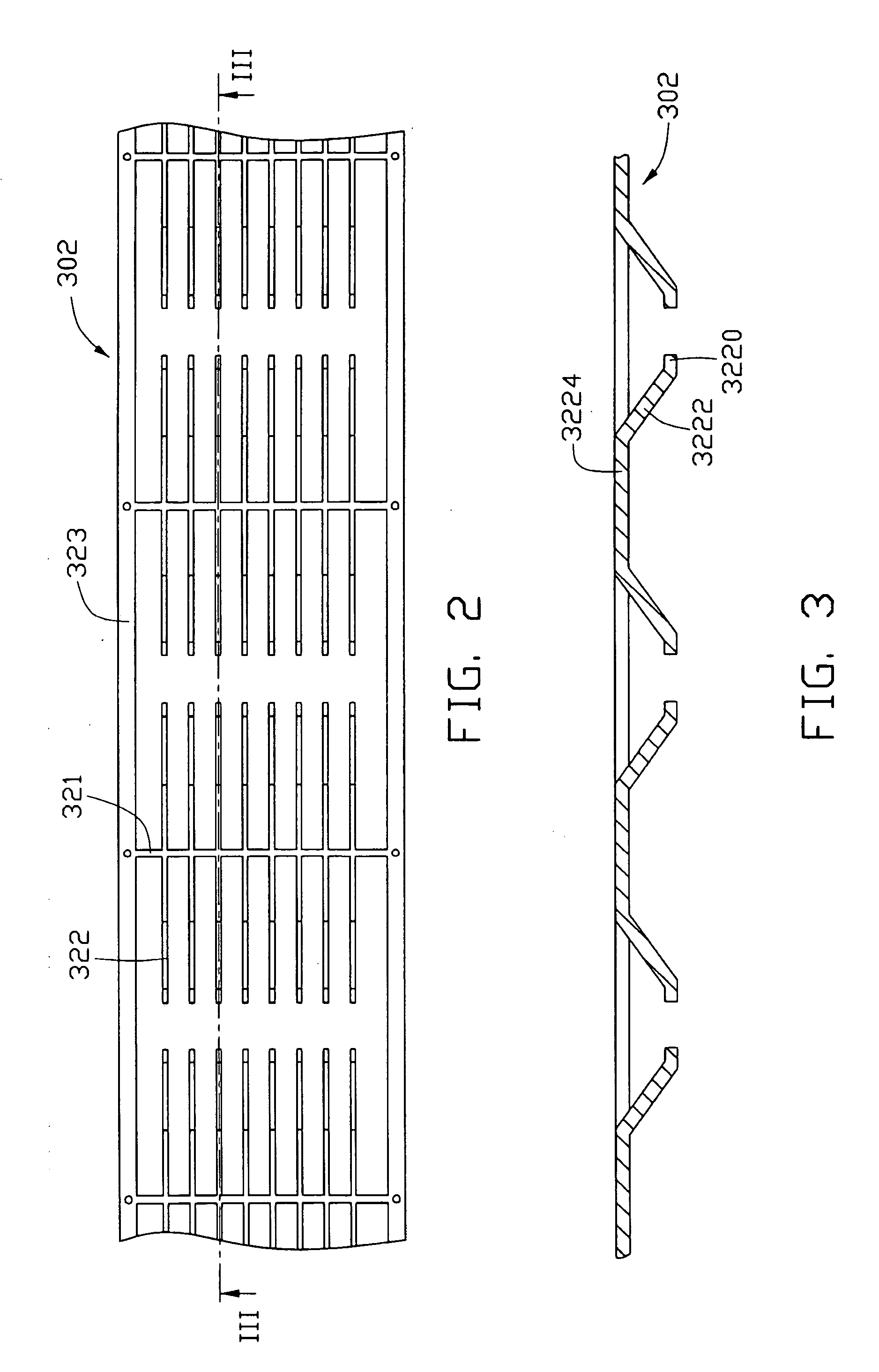
[0025] The carrier 32 of the image sensor chip package 30 includes a number of conductive pieces 322 and a plastic base 324. The conductive pieces 322 are spaced from each other and aligned in parallel, and cooperatively form the carrier 32 when combined with the plastic base 324.

[0026] The image sensor chip 34 is received in the carrier 32, and is adhered to the bottom of the carrier 32 with an adhesive glue 346. A top surface of the image sensor chip 34 is arranged with a photosensitive area 344 and a number of chip pads 342 around the photosensitive area 344.

[0027] The bonding wires 36 can be made of a conductive material such as, for example, gold or aluminum alloy. One end of each wire 36 is connected / joined with a respective chip pad 342 of the image sens...


PUM


Abstract

An image sensor package method includes the steps of first, providing a carrier (30), which includes a base (24) and a leadframe (320). The base has a cavity therein and the leadframe includes a number of conductive pieces; Second, mounting an image sensor chip on the base and received in the cavity, the image sensor having a photosensitive area. Third, providing a plurality of wires, each electrically connects the image sensor chip and a corresponding one of the conductive pieces of the carrier. Fourth, applying an adhesive means around the image sensor chip that at least partially covers all the wires. Finally, mounting a transparent cover on the carrier, where an adhesive means fixes the cover in place.

Description

CROSS-REFERENCE TO RELATED APPLICATIONS [0001] This application is related to a co-pending U.S. Patent Application (Attorney Docket No.US7597), entitled “DIGITAL CAMERA MODULE PACKAGE FABRICATION METHOD”, by Steven Webster et al. Such application has the same assignee as the present application and has been concurrently filed herewith. The disclosure of the above identified application is incorporated herein by reference.TECHNICAL FIELD [0002] The present invention generally relates to an integrated circuit (IC) chip package fabrication method and, more particularly, to an image sensor chip package for use in digital cameras. BACKGROUND [0003] Image sensors are widely used in digital camera modules in order to convert the optical image data of an object into electrical signals. In order to protect the image sensor from contamination or pollution (i.e. from dust or water vapor), the image sensor is generally sealed in a structural package. [0004] A typical image sensor chip package m...

Claims


Application Information

Patent Timeline
IPC IPC(8): H01L27/00
CPCH01L27/14618H01L27/14685H01L27/14683H01L27/14625H01L2224/48091H01L2224/48227H01L2224/73265H01L2924/00014
Inventor WEBSTER, STEVENWU, YING-CHENGLIU, KUN-HSIEH
Owner POLIGHT TECH LTD
Why Eureka
Eureka Blog
Learn More