Method for designing semiconductor apparatus, system for aiding to design semiconductor apparatus, computer program product therefor and semiconductor package

a technology for semiconductor devices and semiconductor packages, applied in the direction of cross-talk/noise/interference reduction, instruments, cad circuit designs, etc., can solve the problems of long design cycle, failure of semiconductor chips to work properly, and no one can identify a problematic section of each semiconductor package, so as to shorten the design cycle of a semiconductor package or a semiconductor apparatus

Inactive Publication Date: 2007-03-15
LONGITUDE SEMICON S A R L
View PDF9 Cites 17 Cited by
  • Summary
  • Abstract
  • Description
  • Claims
  • Application Information

AI Technical Summary

Benefits of technology

[0006] It is an object of the present invention to provide a novel design method which can shorten a design cycle of a semiconductor package or a semiconductor apparatus.

Problems solved by technology

If the above-mentioned voltage fluctuations exceed a certain level, the semiconductor chip fails to function properly.
However, according to the conventional transient analysis, nobody can identify a problematic section of each semiconductor package.
Hence, such design modification is normally carried out multiple times by trial and error, in accordance with the conventional transient analysis, so that its design cycle needs long time.

Method used


Image

  • Method for designing semiconductor apparatus, system for aiding to design semiconductor apparatus, computer program product therefor and semiconductor package
  • Method for designing semiconductor apparatus, system for aiding to design semiconductor apparatus, computer program product therefor and semiconductor package
  • Method for designing semiconductor apparatus, system for aiding to design semiconductor apparatus, computer program product therefor and semiconductor package

Examples


Embodiment Construction

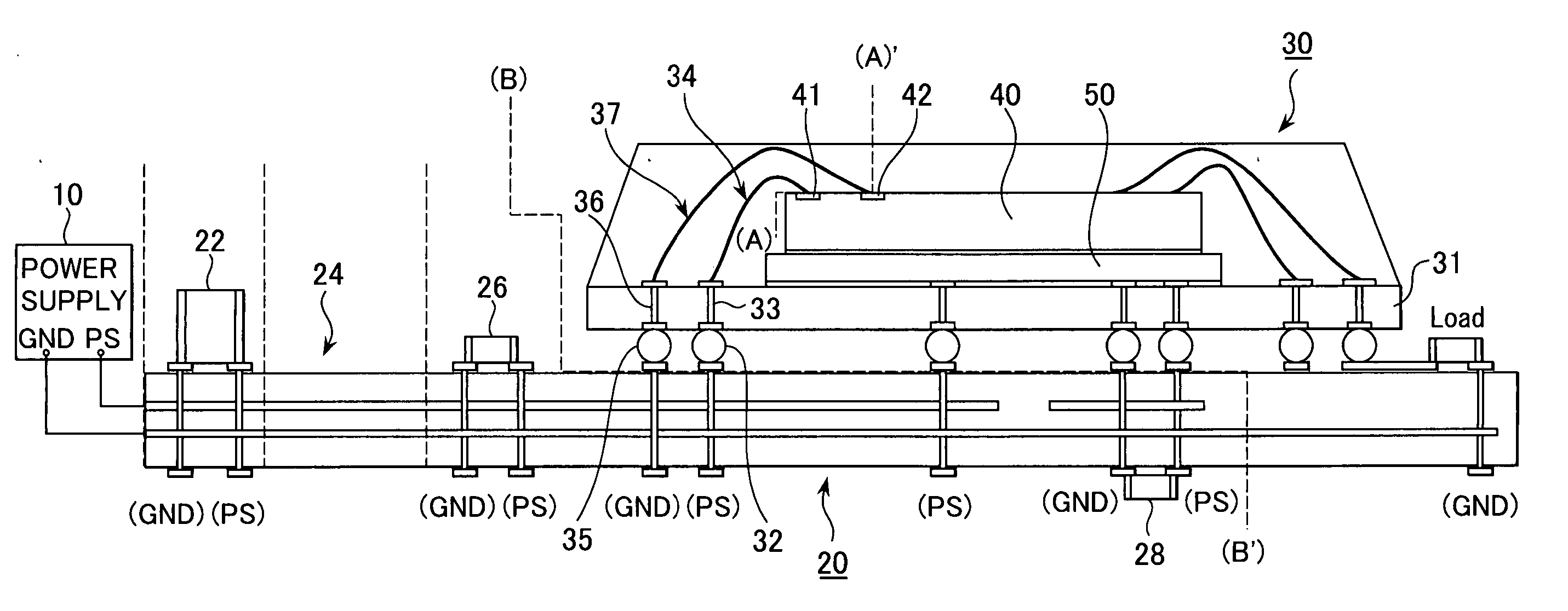
[0029] Explanation will be made about a case where a design method according to a first embodiment of the present invention is applied for designing a semiconductor apparatus shown in FIG. 1.

[0030] With reference to FIG. 1, the semiconductor apparatus comprises a power supply unit 10, a printed circuit board (PCB) 20 and a multi-chip package (MCP) 30. The power supply unit 10 has a power supply portion (PS) and a ground portion (GND). The printed circuit board 20 comprises, as electrical components, a large capacitor 22, a power supply line 24, a bypass capacitor 26, and another bypass capacitor 28. The power supply line 24 is also referred to as a power supply pattern, a set of power supply traces, or a power supply plane. The bypass capacitor 26 is mounted on one surface of the printed circuit board 20, while the other bypass capacitor 28 is mounted the other surface of the printed circuit board 20. The multi-chip package 30 has a structure in which a DRAM chip 40 and a controlle...


PUM


Abstract

A method for designing a semiconductor apparatus comprising a semiconductor package in consideration of power integrity for a semiconductor chip included in the semiconductor package is disclosed. A target variable for an adjustment target is calculated on the basis of target information about the adjustment target, wherein the target variable is represented in frequency domain, and the adjustment target includes a part of the semiconductor package. The target variable is compared with a predetermined constraint, which is represented in frequency domain, to identify a problematic section, wherein the problematic section corresponds to a frequency region at which the target variable exceeds the predetermined constraint. Design guidelines are decided to solve the identified problematic section.

Description

BACKGROUND OF THE INVENTION [0001] This invention relates to a designing method aiming power integrity of a semiconductor chip included in the semiconductor package and to a design aid system and a computer program product in both of which the method is implemented. The invention also relates to a semiconductor package manufactured in accordance with the method. [0002] In a semiconductor chip such as a dynamic random access memory (DRAM) chip, transient currents flow at a power supply pad and a ground pad of the semiconductor chip, for example, when an output driver of the semiconductor chip changes its output state, i.e. from high level to low level, or from low level to high level. The transient currents cause voltage fluctuations at the power supply pad and the ground pad. [0003] If the above-mentioned voltage fluctuations exceed a certain level, the semiconductor chip fails to function properly. Therefore, each semiconductor package including the semiconductor chip should be des...

Claims


Application Information

Patent Timeline
Patent Type & Authority Applications(United States)
IPC IPC(8): H01L23/48
CPCG06F17/5068H05K1/0231H05K3/0005H05K2201/10545H01L2224/49175H01L2924/15311H01L2224/73265H01L2224/48091H01L2224/48227H05K2201/10734H01L2924/00014G06F30/39H01L2224/05553H01L2224/2612H01L2924/181H01L2924/3011H01L2924/00H01L2924/00012
Inventor KATAGIRI, MITSUAKINAKAMURA, SATOSHISUGA, TAKASHIISA, SATOSHINISHIO, YOJIFUNABA, SEIJIHIROSE, YUKITOSHI
Owner LONGITUDE SEMICON S A R L
Why Eureka
Try Eureka