Pixel circuit, display unit, and pixel circuit drive method

a pixel circuit and display unit technology, applied in the direction of static indicating devices, pulse techniques, instruments, etc., can solve the problems of deterioration of i-v characteristics of organic el elements, fluctuation of operating points, and difficulty in realizing large-scale high-definition displays, etc., to achieve no deterioration of luminance

Active Publication Date: 2007-03-15
SONY CORP
View PDF8 Cites 195 Cited by
  • Summary
  • Abstract
  • Description
  • Claims
  • Application Information

AI Technical Summary

Benefits of technology

[0043] An object of the present invention is to provide a pixel circuit, display device, and method of driving a pixel circuit enabling source-follower output with no deterioration of luminance even with a change of the current-voltag...

Problems solved by technology

While the former has a simple structure, it has the problem that realization of a large sized and high definition display is difficult.
However, here too, similarly, the I-V characteristic of the organic EL element ...

Method used


Image

  • Pixel circuit, display unit, and pixel circuit drive method
  • Pixel circuit, display unit, and pixel circuit drive method
  • Pixel circuit, display unit, and pixel circuit drive method

Examples


first embodiment

[0121]FIG. 8 is a block diagram of the configuration of an organic EL display device employing pixel circuits according to the first embodiment.

[0122]FIG. 9 Is a circuit diagram of the concrete configuration of a pixel circuit according to the first embodiment in the organic EL display device of FIG. 8.

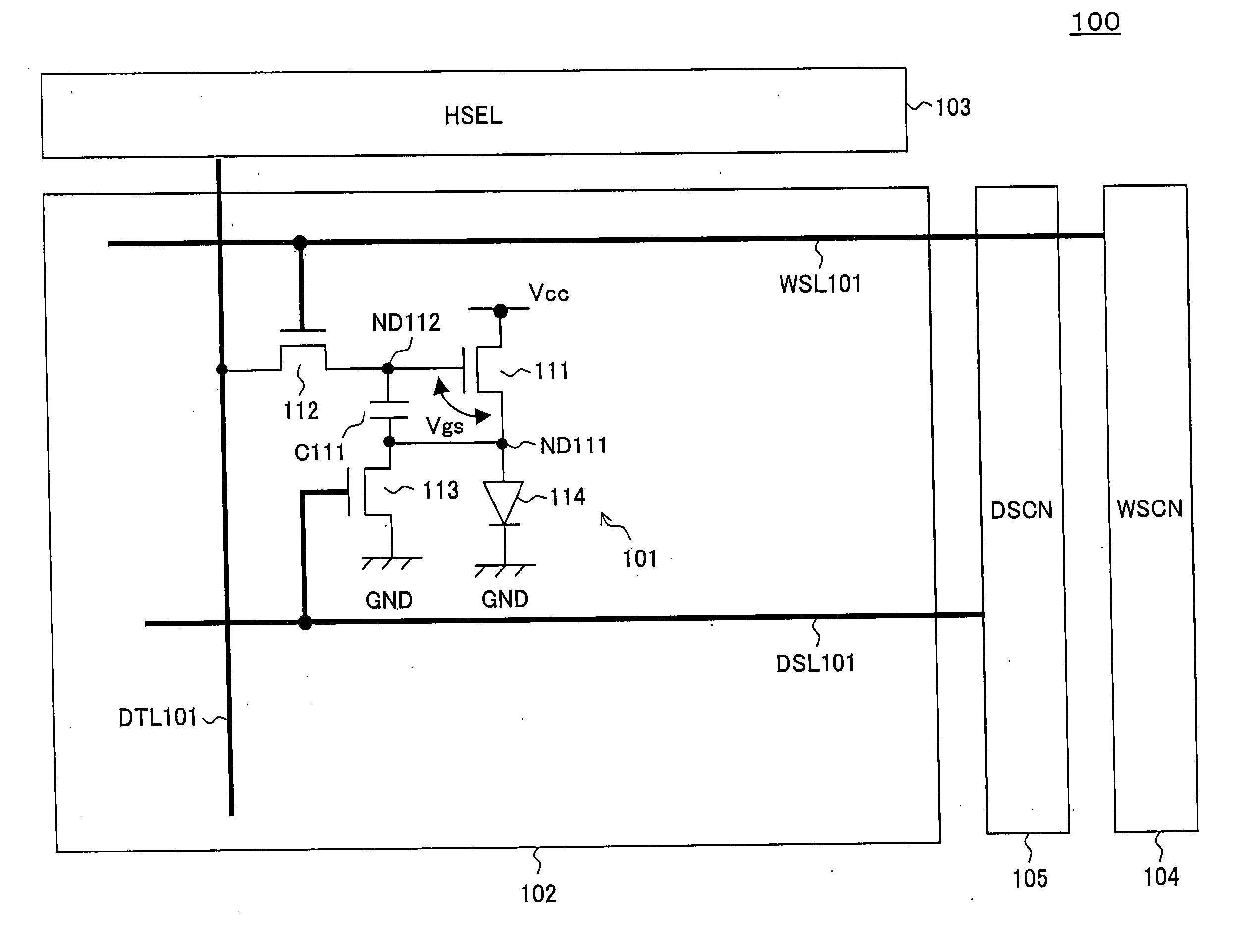
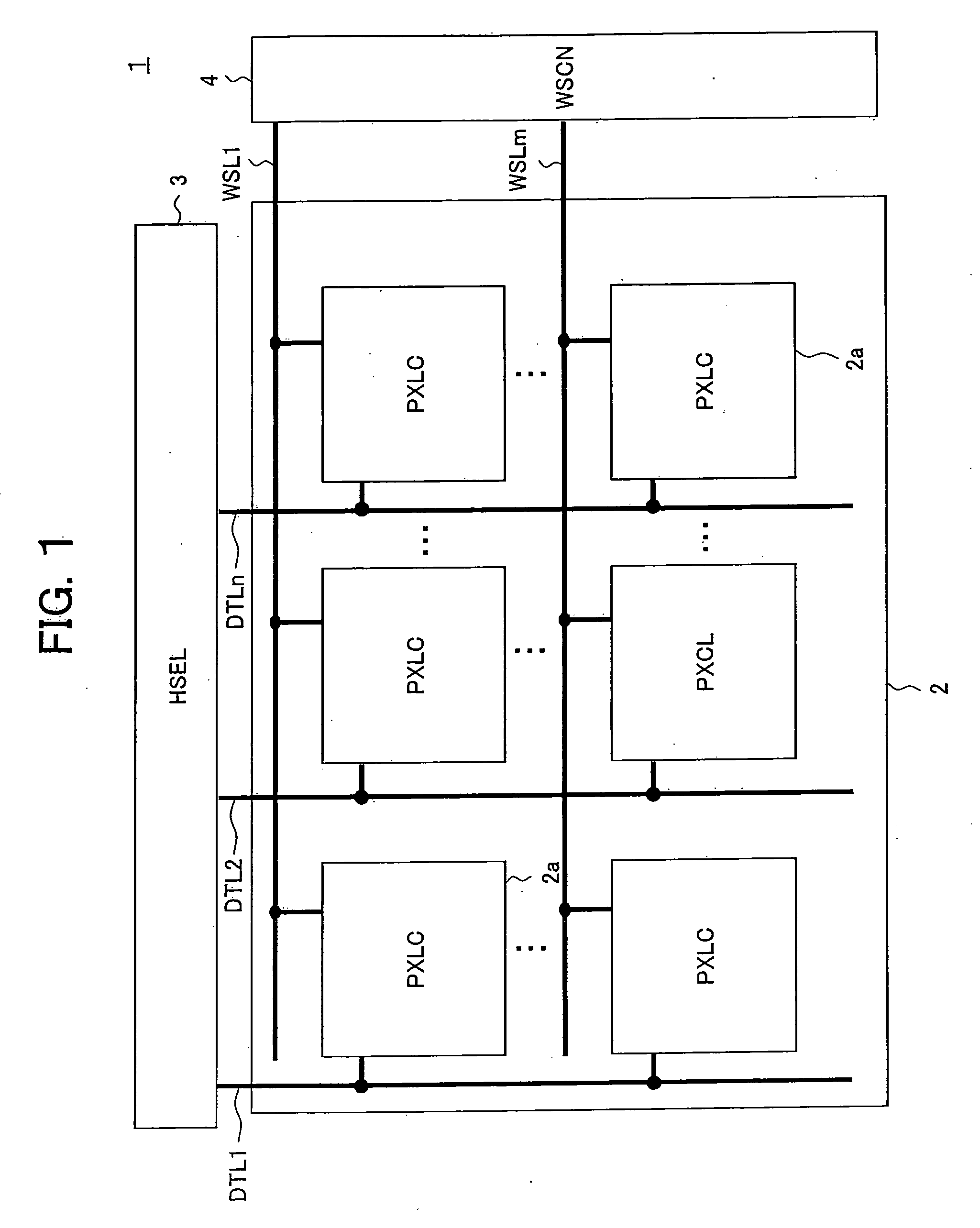
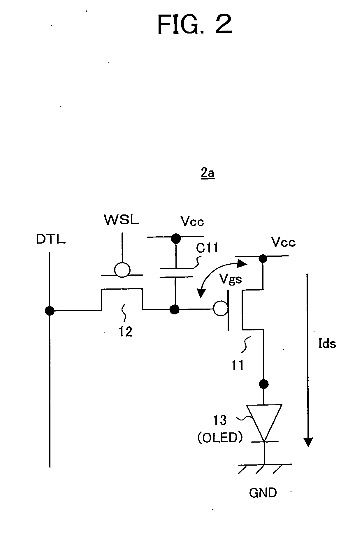
[0123] This display device 100 has, as shown in FIG. 8 and FIG. 9, a pixel array portion 102 having pixel circuits (PXLC) 101 arranged in an m×n matrix, a horizontal selector (HSEL) 103, a write scanner (WSCN) 104, a drive scanner (DSCN) 105, data lines DTL101 to DTL10n selected by the horizontal selector 103 and supplied with a data signal in accordance with the luminance information, scanning lines WSL101 to WSL10m selectively driven by the write scanner 104, and drive lines DSL101 to DSL10m selectively driven by the drive scanner 105.

[0124] Note that while the pixel circuits 101 are arranged in an m×n matrix in the pixel array portion 102, FIG. 9 shows an example wherein the pix...

second embodiment

[0161]FIG. 12 is a block diagram of the configuration of an organic EL display device employing pixel circuits according to a second embodiment.

[0162]FIG. 13 is a circuit diagram of the concrete configuration of a pixel circuit according to the second embodiment in the organic EL display device of FIG. 12.

[0163] The display device 200, as shown in FIG. 12 and FIG. 13, has a pixel array portion 202 having pixel circuits (PXLC) 201 arranged in an m×n matrix, a horizontal selector (HSEL) 203, a write scanner (WSCN) 204, a drive scanner (DSCN) 205, data lines DTL201 to DTL20n selected by the horizontal selector 203 and supplied with a data signal in accordance with the luminance information, scanning lines WSL201 to WSL20m selectively driven by the write scanner 204, and drive lines DSL201 to DSL20m selectively driven by the drive scanner 205.

[0164] Note that while the pixel circuits 201 are arranged in an m×n matrix in the pixel array portion 202, FIG. 12 shows an example wherein th...

third embodiment

[0215]FIG. 17 is a block diagram of the configuration of an organic EL display device employing a pixel circuit according to a third embodiment.

[0216]FIG. 18 is a circuit diagram of the concrete configuration of a pixel circuit according to the third embodiment in the organic EL display device of FIG. 17.

[0217] The display device 200A according to the third embodiment differs from the display device 200 according to the second embodiment in the position of connection of the capacitor C211 as the pixel capacitor Cs in the pixel circuit.

[0218] Specifically, in the pixel circuit 201 according to the second embodiment, the capacitor C211 is connected between the gate of the TFT 211 as the drive transistor and the anode side of the EL light emitting element 214.

[0219] As opposed to this, in the pixel circuit 201A according to the third embodiment, the capacitor C211 is connected between the gate and source of the TFT 211 as the drive transistor. Specifically, a first electrode of the...


PUM


Abstract

A pixel circuit, display device, and method of driving a pixel circuit enabling source-follower output with no deterioration of luminance even with a change of the current-voltage characteristic of the light emitting element along with elapse, enabling a source-follower circuit of n-channel transistors, and able to use an n-channel transistor as an EL drive transistor while using current anode-cathode electrodes, wherein a source of a TFT 111 as a drive transistor is connected to an anode of a light emitting element 114, a drain is connected to a power source potential VCC, a capacitor C111 is connected between a gate and source of the TFT 111, and a source potential of the TFT 111 is connected to a fixed potential through a TFT 113 as a switching transistor.

Description

TECHNICAL FIELD [0001] The present invention relates to a pixel circuit having an electro-optic element with a luminance controlled by a current value in an organic EL (electroluminescence) display etc., an image display device comprised of such pixel circuits arrayed in a matrix, in particular a so-called active matrix type image display device controlled in value of current flowing through the electro-optic elements by insulating gate type field effect transistors provided inside the pixel circuits, and a method of driving a pixel circuit. BACKGROUND ART [0002] In an image display device, for example, a liquid crystal display, a large number of pixels are arranged in a matrix and the light intensity is controlled for every pixel in accordance with the image information to be displayed so as to display an image. [0003] This same is true for an organic EL display etc. An organic EL display is a so-called self-light emitting type display having a light emitting element in each pixel ...

Claims


Application Information

Patent Timeline
IPC IPC(8): G09G3/30H01L51/50G09G3/20H01L21/8234H01L27/06H01L27/088H01L29/786H03K17/687H05B33/14H05B44/00
CPCG09G3/3233G09G2300/043G09G2300/0809G09G2300/0819G09G2300/0842G09G2300/0861G09G3/3258G09G3/30G09G3/3426G09G3/36G09G3/3648G09G2320/0233H05B33/0896G09G2320/043G09G2310/0256G09G3/20H05B45/60G09G2320/045
Inventor UCHINO, KATSUHIDEYAMASHITA, JUNICHIYAMAMOTO, TETSURO
Owner SONY CORP
Why Eureka
Try Eureka