Pixel circuit and display device

a display device and pixel technology, applied in the field of pixels, can solve the problems of difficult realization of large sized and high definition displays, difficulty in achieving high-definition displays, and difficulty in the current level of technology, so as to prevent overlap, reduce resistance, and reduce resistance

Active Publication Date: 2005-01-20
SONY CORP
View PDF4 Cites 36 Cited by
  • Summary
  • Abstract
  • Description
  • Claims
  • Application Information

AI Technical Summary

Benefits of technology

[0035] A first object of the present invention is to provide a pixel circuit able to prevent a spread of the terminal voltages of drive transistors inside a panel and in turn able to reliably prevent deterioration of uniformity and a display device for the same.
[0036] A second object of the present invention is to provide a pixel circuit able to reliably prevent deterioration of the uniformity, enabling source-follower output with no deterioration of luminance even with a change of the current-voltage characteristic of the light emitting element along with time, enabling a source-follower circuit of n-channel transistors, and able to use an n-channel transistor as an EL drive transistor while using current anode-cathode electrodes and a display device for the same.
[0049] According to the present invention, since the power source voltage source interconnects and the reference power source interconnects are laid out in the same direction so as not to have any intersecting parts, it is possible to prevent overlap between the power source voltage source interconnects and the reference power source interconnects. Accordingly, it is possible to lay out the reference power source interconnects (Vss interconnects) by a lower resistance than the past. Further, the number of pixels connected to a single interconnect is smaller in the vertical direction (y-direction) than the horizontal direction (x-direction) at a general angle of view, so with the same line width, it is possible to lay out the reference power source interconnects by a lower resistance than the past.
[0050] According to the present invention, further, since the source electrode of a drive transistor is connected to a fixed potential through a switch and there is a pixel capacity between the gate and source of the drive transistor, the change in luminance due to the change in the I-V characteristic of a light emitting element along with time is corrected. When the drive transistor is an n-channel transistor, by making the fixed potential a ground potential, the potential applied to the light emitting element is made the ground potential so as to create a non-emitting period of the light emitting element. Further, by adjusting the off period of the second switch connecting the source electrode and ground potential, the emitting and non-emitting periods of the light emitting element are adjusted for duty driving. Further, by making the fixed potential close to the ground potential or a potential lower than that or by raising the gate voltage, deterioration of the image quality due to fluctuation in the threshold voltage Vth of the switch transistor connected to the fixed potential is suppressed. Further, when the drive transistor is a p-channel transistor, by making the fixed potential the potential of the power source connected to the cathode electrode of the light emitting element, the potential applied to the light emitting element is made the power source potential so as to create a non-emitting period of the organic EL element. Further, by making the characteristic of the drive transistor an n-channel type, a source-follower circuit becomes and anodic connection becomes possible. Further, making all of the drive transistors n-channel transistors becomes possible, introduction of a general amorphous silicon process becomes possible, and reduction of the cost becomes possible.
[0051] Further, since the second switch is laid out between the light emitting element and the drive transistor, current is not supplied to the drive transistor in the non-emitting period and therefore power consumption of the panel is suppressed. Further, by using a potential of the cathode side of the light emitting element as the ground potential, for example, the second reference potential, there is no need to provide a GND interconnect at the TFT side inside the panel. Further, by being able to delete the GND interconnects of the TFT substrates in the panel, layout in the pixels and layout of the peripheral circuits become easy. Further, by being able to delete the GND interconnects of the TFT substrates in the panel, there is no overlap between the power source potential (first reference potential) and ground potential (second reference potential) of the peripheral circuits, the Vcc lines can be laid out with a lower resistance, and a high uniformity can be achieved.
[0052] Further, by turning the third switch at the power source interconnect side on when writing in a signal line so as to lower the impedance, the coupling effect on pixel writing is corrected in a short time and an image of a high uniformity is obtained.

Problems solved by technology

An organic EL display, in the same way as a liquid crystal display, may be driven by a simple matrix and an active matrix system, but while the former has a simple structure, it has the problem that realization of a large sized and high definition display is difficult.
This is considered extremely difficult with the current level of technology.
However, this method of the related art had problems.
When this fluctuation entered the ground line during the signal sampling period, the gate-source voltage Vgs of the drive transistor constituted by the TFT 41 ended up with a spread in the panel and as a result the uniformity ended up deteriorating.

Method used


Image

  • Pixel circuit and display device
  • Pixel circuit and display device
  • Pixel circuit and display device

Examples


first embodiment

[0073] First Embodiment

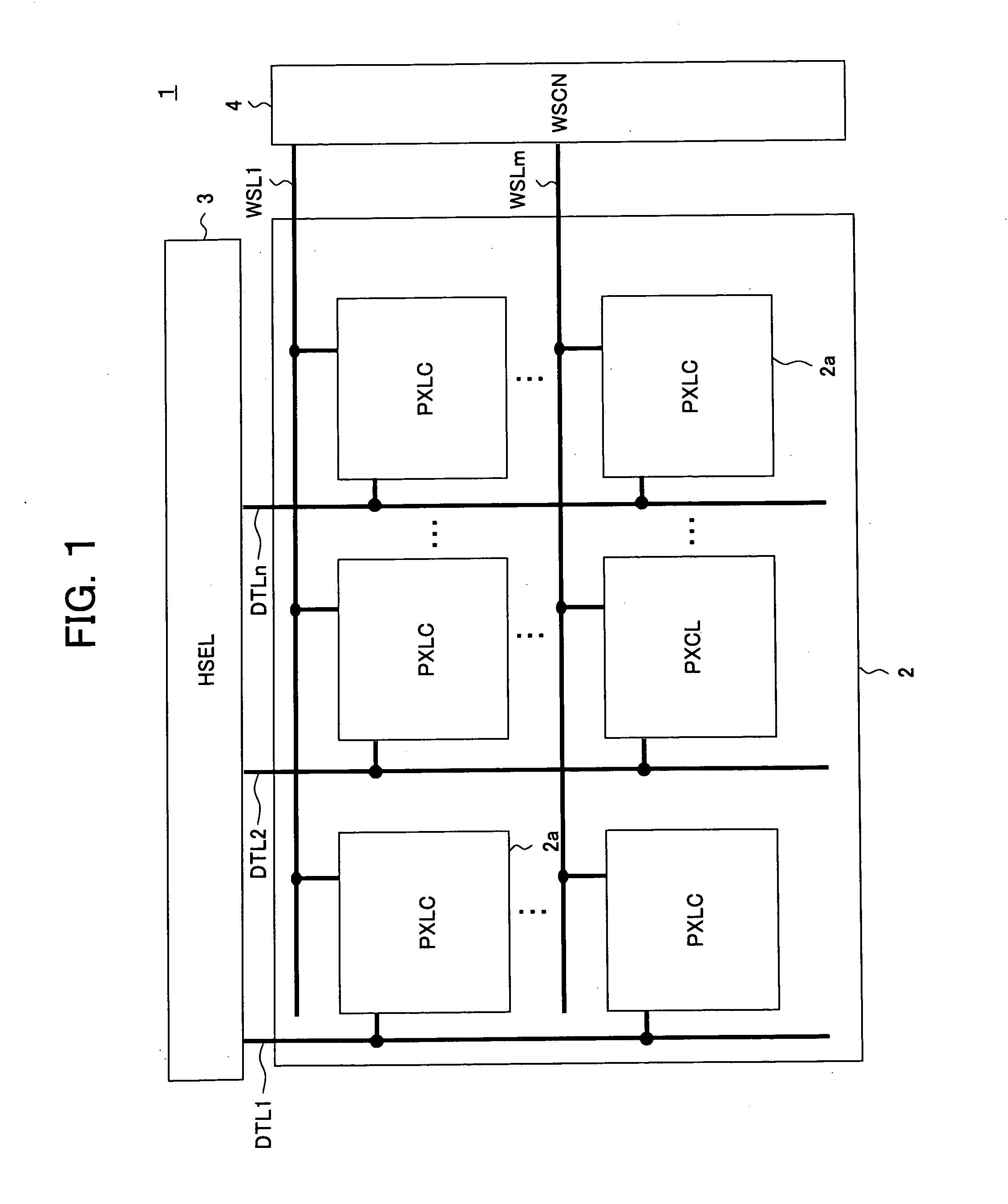
[0074]FIG. 10 is a block diagram of the configuration of an organic EL display device employing pixel circuits according to the first embodiment. FIG. 11 is a circuit diagram of the concrete configuration of a pixel circuit according to the first embodiment in the organic EL display device of FIG. 10.

[0075] This display device 100 has, as shown in FIG. 10 and FIG. 11, a pixel array portion 102 having pixel circuits (PXLC) 101 arranged in an m×n matrix, a horizontal selector (HSEL) 103, a write scanner (WSCN) 104, a drive scanner (DSCN) 105, data lines DTL101 to DTL10n selected by the horizontal selector 103 and supplied with a data signal in accordance with the luminance information, scanning lines WSL101 to WSL10m selectively driven by the write scanner 104, and drive lines DSL101 to DSL10m selectively driven by the drive scanner 105.

[0076] Note that while the pixel circuits 101 are arranged in an m×n matrix in the pixel array portion 102, FIG. 11 shows an ...

second embodiment

[0092] Second Embodiment

[0093]FIG. 15 is a block diagram of the configuration of an organic EL display device employing pixel circuits according to a second embodiment. FIG. 16 is a circuit diagram of the concrete configuration of a pixel circuit according to the second embodiment in the organic EL display device of FIG. 15.

[0094] The display device 200, as shown in FIG. 15 and FIG. 16, has a pixel array portion 202 having pixel circuits (PXLC) 201 arranged in an m×n matrix, a horizontal selector (HSEL) 203, a first write scanner (WSCN1) 204, a second write scanner (WSCN2) 205, a drive scanner (DSCN) 206, data lines DTL201 to DTL20n selected by the horizontal selector 203 and supplied with a data signal in accordance with the luminance information, scanning lines WSL201 to WSL20m selectively driven by the write scanner 204, scanning lines WSL211 to WSL21m selectively driven by the write scanner 205, and drive lines DSL201 to DSL20m selectively driven by the drive scanner 206.

[0095...


PUM


Abstract

A pixel circuit able to prevent a spread of the terminal voltages of drive transistors inside a panel and in turn able to reliably prevent deterioration of uniformity, wherein a source of a TFT serving as a drive transistor is connected to an anode of a light emitting element, a drain is connected to a power source potential, a capacitor is connected between a gate and source of the TFT, and a source potential of the TFT is connected to a fixed potential through a TFT serving as a switch transistor and wherein pixel circuit lines are connected by an upper line and bottom line and are arranged in parallel with pixel circuit power source voltage lines so as not to have intersecting parts.

Description

BACKGROUND OF THE INVENTION [0001] 1. Field of the Invention [0002] The present invention relates to a pixel circuit having an organic electroluminescence (EL) element or other electro-optic element with a luminance controlled by a current value and an image display device comprised of such pixel circuits arrayed in a matrix, in particular a so-called active matrix type image display device controlled in value of current flowing through the electro-optic elements by insulating gate type field effect transistors (FETs) provided inside the pixel circuits. [0003] 2. Description of the Related Art [0004] In an image display device, for example, a liquid crystal display, a large number of pixels are arranged in a matrix and the light intensity is controlled for every pixel in accordance with the image information to be displayed so as to display an image. This same is true for an organic EL display etc. An organic EL display is a so-called self light emitting type display having a light ...

Claims


Application Information

Patent Timeline
Patent Type & Authority Applications(United States)
IPC IPC(8): H01L51/50G09F9/30G09G3/20G09G3/30G09G5/00H03K17/16H03K17/693H03K19/00H05B33/14
CPCG09G3/3233G09G2300/0417G09G2300/0426G09G2300/043G09G3/3208G09G2300/0842G09G2300/0861G09G2310/0256G09G2320/043G09G2300/0819G09G3/30G09G2300/0439G09G2330/028G09G3/3266
Inventor UCHINO, KATSUHIDEYAMASHITA, JUNICHIYAMAMOTO, TETSURO
Owner SONY CORP
Why Eureka
Try Eureka