Image sensing device package structure

a sensing device and package technology, applied in the direction of instruments, photoelectric discharge tubes, electric discharge lamps, etc., can solve the problems of reducing the application range limiting the package and affecting the application of portable products. , to achieve the effect of shrinking the area and volume of the package structur

Inactive Publication Date: 2007-03-22
SIGURD MICROELECTRONICS CORP
View PDF8 Cites 3 Cited by
  • Summary
  • Abstract
  • Description
  • Claims
  • Application Information

AI Technical Summary

Benefits of technology

[0006] An object of the present invention is to provide an image sensing device package structure, in which wire bonding positions of an image sensing device are changed to shorten the wire bonding pitch for reducing the package area, thereby accomplishing a miniaturized package of the image sensing device.
[0007] To achieve the above object, an image sensing device package structure of the present invention comprises an image sensing device, a base, and a light transparent layer. The base has an upper surface and a lower surface. Several metallization traces are provided on the upper and lower surfaces. More than one bonding wire is used to connect the metallization traces on the upper surface with the image sensing device. The horizontal height of the top of the metallization traces on the upper surface is slightly larger than that of the top of the image sensing device to reduce the wire bonding pitch of bonding wire. The light transparent layer covers on the upper surface of the base.
[0010] Furthermore, in the above embodiment, the difference between the horizontal heights of the third upper surface and the second upper surface of the base can decrease to prevent the capillary tip from touching the edge of the base when performing bonding wire ball bonding. The required length of the second upper surface of the base can thus be reduced to shrink the area and volume of the package structure.

Problems solved by technology

The above conventional package structure, however, has a primary drawback, Because the image sensing device 30 has a height different with respect to the substrate 10 during wire bonding, a corresponding wire bonding pitch S1 is required.
Therefore, there is much limit in the package area and volume of this package structure, hence being adverse to applications in portable products.

Method used


Image

  • Image sensing device package structure
  • Image sensing device package structure
  • Image sensing device package structure

Examples


Embodiment Construction

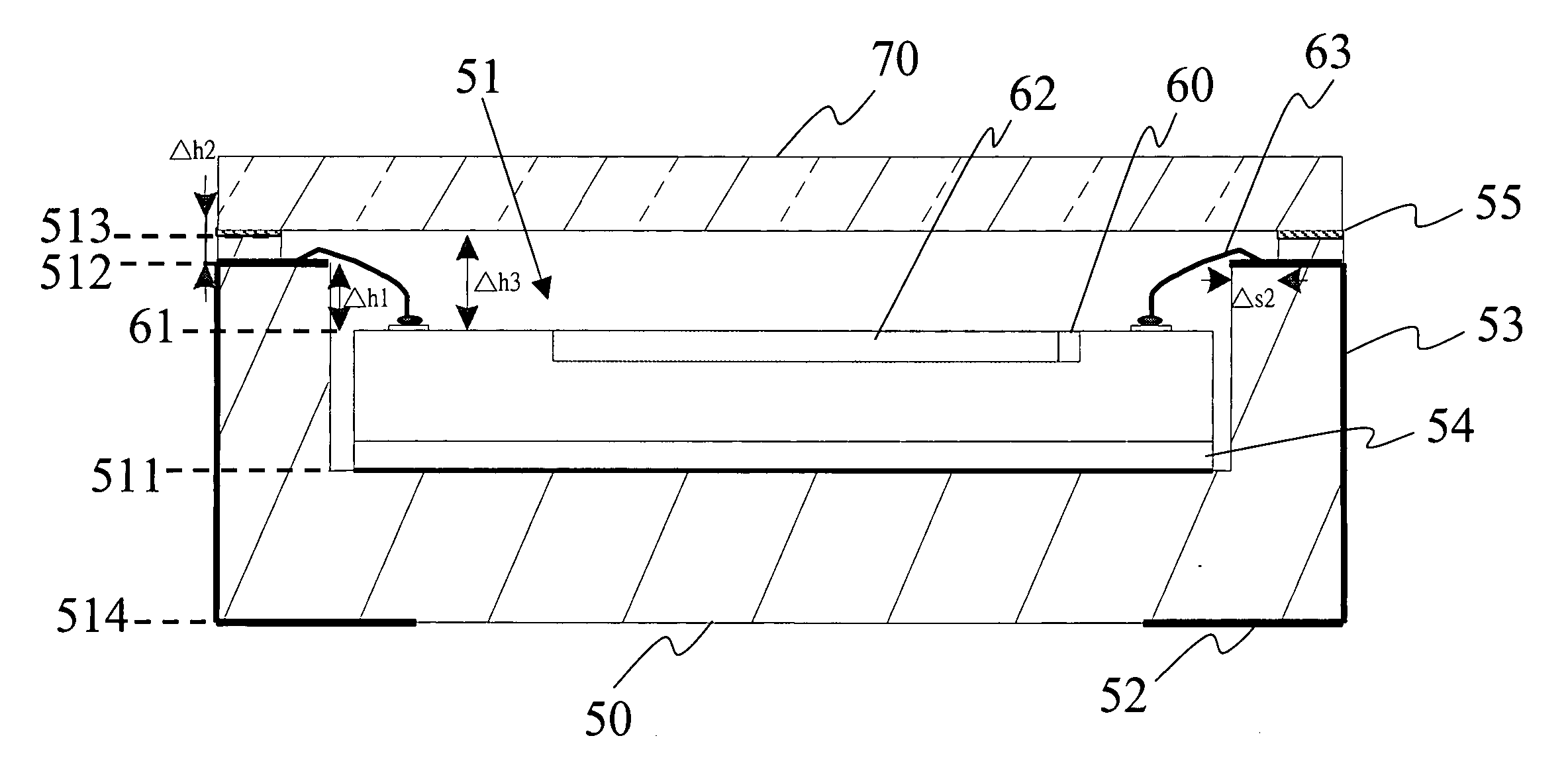
[0017] As shown in FIG. 2, an image sensing device package structure of the present invention comprises a base 50, an image sensing device 60, and a light transparent layer 70. The base 50 can be made of ceramic material. A groove 51 is formed on the upper surface of the base 50. A first upper surface 511 is formed at the bottom of the groove 51. The edge of the groove 51 has a difference in height to form a second upper surface 512 and a third upper surface 513 having different horizontal heights. The horizontal height of the second upper surface 512 is larger than that of the first upper surface 511. The horizontal height of the third upper surface 513 is larger than that of the second upper surface 512. Several metallization traces 52 are disposed on the second upper surface 512 and a lower surface 514 of the base 50. The metallization traces 52 on the second upper surface 512 and a lower surface 514 are electrically connected together via a shaped metallization trace 53 at the o...


PUM


Abstract

An image sensing device package structure is formed by using a base and a light transparent layer to package an image sensing device. The image sensing device is electrically connected to metallization traces on the base by means of wire bonding. Through change of the positions of the metallization traces, contacts between bonding wires and the metallization traces are made slightly higher than the top of the image sensing device, thereby shortening the wire bonding pitch of the bonding wires and thus reducing the package area.

Description

BACKGROUND OF THE INVENTION [0001] 1. Field of the Invention [0002] The present invention relates to an image sensing device package structure and, more particularly, to an image sensing device package structure capable of reducing the package area. [0003] 2. Description of Related Art [0004] As shown in FIG. 1, a conventional CMOS image sensing device package structure comprises a substrate 10, a frame 20, an image sensing device 30, and a light transparent glass 40. Several metallization traces 11 are provided on the surface of the substrate 10. The frame 20 is adhered to the substrate 10 using a first glue layer 12. The image sensing device 30 adheres to the substrate 10. The image sensing device 30 has an image sensing area 31. The image sensing device 30 is connected to the metallization traces 11 on the surface of the substrate 10 via bonding wires 32 by means of wire bonding to achieve electric connection between the image sensing device 30 and the substrate 10. The light tra...

Claims


Application Information

Patent Timeline
Patent Type & Authority Applications(United States)
IPC IPC(8): H01J40/14
CPCH01L23/057H01L27/14618H01L2924/12041H01L2224/32225H01L24/48H01L2924/16195H01L2924/15153H01L2924/01077H01L2224/73265H01L2224/48227H01L2224/48091H01L2924/00014H01L2924/00H01L2924/00012H01L24/73H01L2224/48465H01L2224/45099H01L2224/45015H01L2924/207
Inventor CHEN, PO-HUNG
Owner SIGURD MICROELECTRONICS CORP
Why Eureka
Try Eureka