
Displacement detection device

a displacement detection and detection device technology, applied in microstructural devices, microstructures, instruments, etc., can solve the problems of displacement detection devices that have an operation problem, difficult to miniaturize an acceleration sensor apparatus in such a structure, and difficult to satisfy both good sensitivity and good impact resistance, so as to achieve high reliability and reduce the loss of chipping on the side ridge of ic chips.

Inactive Publication Date: 2007-03-22
HITACHI METALS LTD
View PDF3 Cites 5 Cited by
  • Summary
  • Abstract
  • Description
  • Claims
  • Application Information

AI Technical Summary

Benefits of technology

The present invention provides an IC chip for a displacement detection device that does not have loose chippings, and a protection case for the device. The IC chip has grinding traces on its rear surface that are angled to prevent excessive deformation of the chip. The invention also includes a displacement detection device comprising the IC chip and a protection case. The grinding traces on the rear surface of the IC chip are angled at an angle of 0 to 45 degrees with a vertical line on the side ridge of the chip. This reduces the appearance ratio of loose chippings and the use of adhesive to bond the chip to the detection element. The invention is particularly useful for flexible detection devices that use a rectangular IC chip with grinding traces on the rear surface angled at an angle of 0 to 20 degrees with a vertical line on the side ridge of the chip.

Problems solved by technology

But, it is hard to miniaturize an acceleration sensor apparatus in such a structure.
It is difficult to satisfy both the good sensitivity and the good impact resistance.
However, among a number of displacement detection devices manufactured, displacement detection devices that have an operation problem due to silicon broken pieces caused from IC chips have occurred, though it was a very low happening frequency.
Silicon broken pieces caused from the IC chip are confined in the protection case, move around in the protection case, and are trapped into gaps between the flexibly deformable portion of the displacement detection element and the IC chip, and the trapped silicon broken pieces obstruct the movement of the flexibly deformable portions.
Chippings at issue are loose chippings, which remain at defected portions, that is, silicon broken pieces partially held by the IC substrates.
During assembling and / or using the displacement detection devices, silicon broken pieces drop from loose chippings and affect properties of the displacement detection devices.

Method used


Image

  • Displacement detection device
  • Displacement detection device
  • Displacement detection device

Examples


example 1

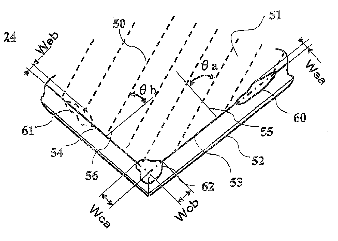
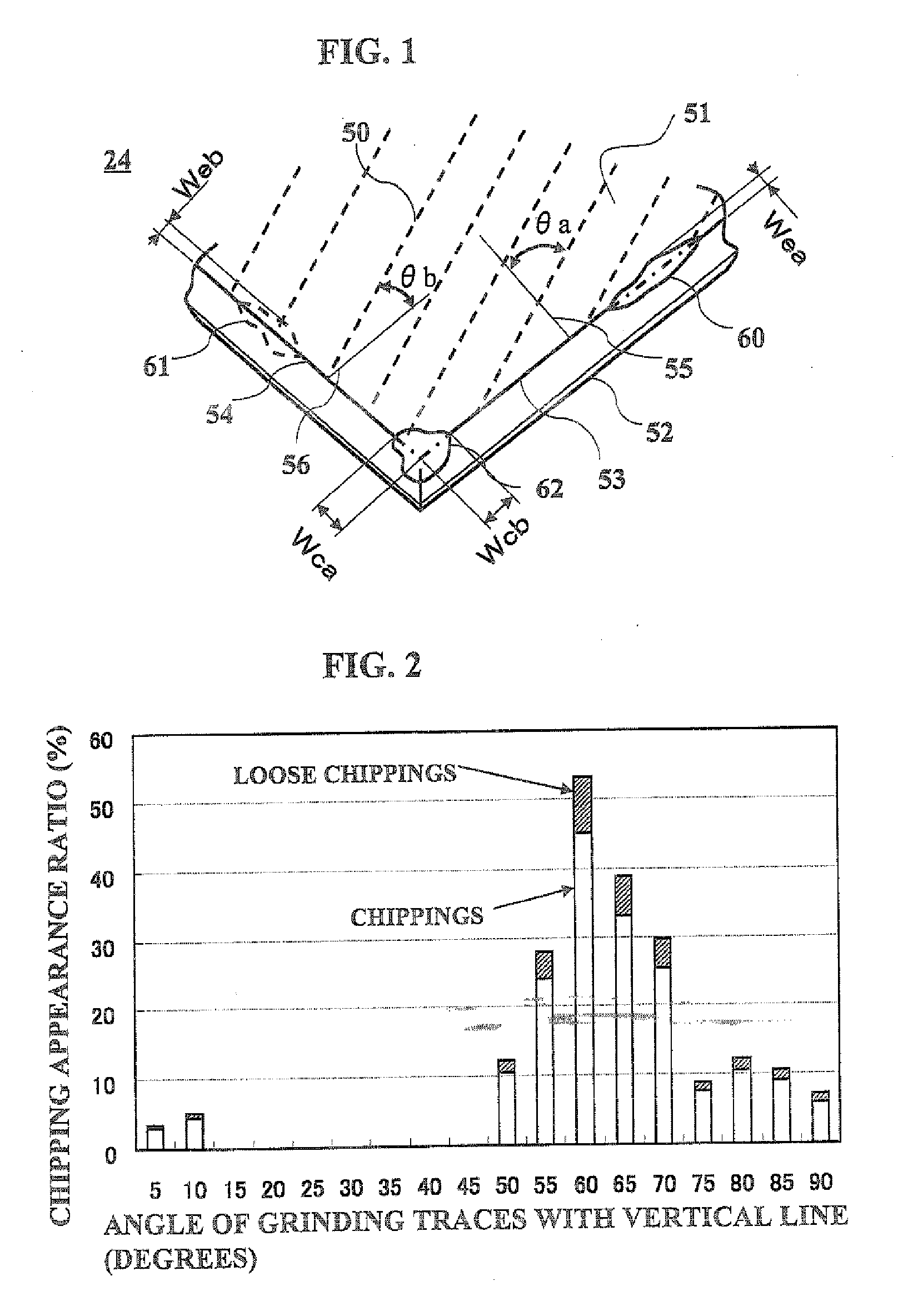
[0037] A relationship between an angle of grinding traces with a dicing direction of IC wafers and chipping appearance frequency will be explained below. First of all, methods of grinding and dicing and conditions for taking data are described. After reducing thickness of IC wafers from 625 μm to 250 μm in silicon thickness by grinding, the wafers were cut into IC chips of 2.6 mm×2.2 mm by a diamond dicing wheel. A waterproof sheet was bonded onto an IC circuit surface to protect the IC circuit from a grinding coolant for grinding. The grinding was done by a rotary grinding machine with a diamond grinding wheel of #2000 at a revolution speed of about 600 rpm. The surface roughness of the ground surface was 0.13 μm in Rmax and 0.014 μm in Ra. Rmax and Ra were measured according to JIS B 0601. Since a thickness of the IC circuit was about 5 μm, the thickness to cut was about 255 μm. The IC wafer was bonded to an adhesive sheet, and the IC wafer was diced until a half of the adhesive s...

example 2

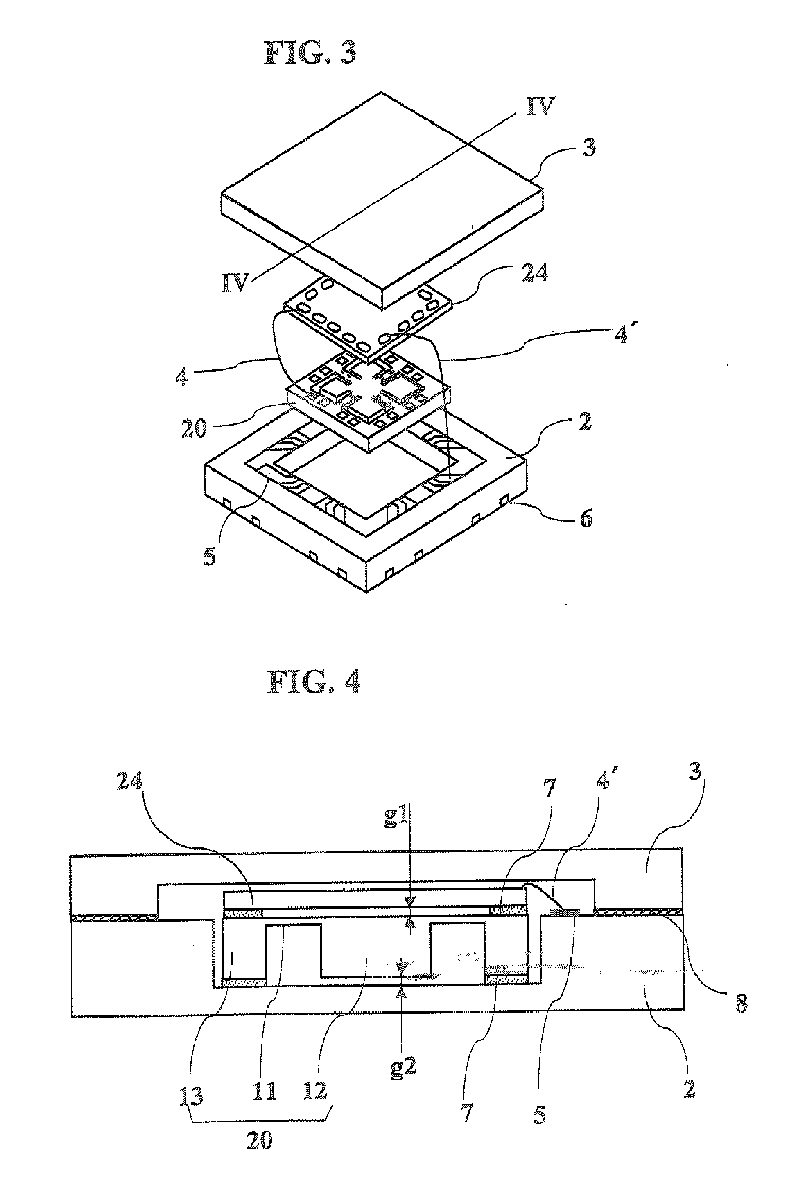
[0044] Using IC chips having loose chippings, acceleration sensors that are a kind of displacement detection devices were assembled. An exploded perspective view of the assembled acceleration sensor is shown in FIG. 3. In FIG. 3, an acceleration sensor element 20 is electrically connected to an IC chip 24 by lead wires 4, and the IC chip 24 is connected by wires 4′ to terminals 5 of a protection case 2 and to external terminals 6. An acceleration sensor 10 is assembled with a protection case lid 3 fixed on and sealed with the protection case 2. Piezo resistors of the acceleration sensor element 20 are omitted from the drawing, FIG. 4 shows a cross-sectional view taken along the line IV-IV of FIG. 3. The acceleration sensor element 20 is composed of a weight 12, a support frame 13 and flexibly deformable portions 11. Piezo resistors (not shown) connected with the lead wires 4 are formed on surfaces of the flexibly deformable portions 11. The IC chip 24 is disposed for a rear surface ...

example 3

[0050]FIG. 5A and FIG. 5B show acceleration sensor elements for acceleration sensors of EXAMPLE 3 by perspective views. An IC chip 24′ is fixed on an acceleration sensor element 20 in FIG. 5A with three side ridges of the rectangular IC chip 24′ bonded to a support frame by adhesive 7′. On the top surface of the IC chip 24′, an IC circuit is formed, and a rear surface (a surface facing the acceleration sensor element 20) of the IC chip 24′ is ground to have a predetermined thickness in the same manner as shown in FIG. 1 and grinding traces at an angle of 15 degrees to 30 degrees with a vertical line on the side ridge 53. The side ridge 53 having the grinding traces at the angle of 15 degrees to 30 degrees with the vertical line does not have chippings on it, as explained in EXAMPLE 1. Since side ridges 54 perpendicular to the side ridge 53 have grinding traces at an angle of 75 degrees to 60 degrees with a vertical line, the side ridges 54 show loose chipping appearance ratio of 5 t...


PUM


Abstract

In a displacement detection device having an IC chip for a regulation plate, silicon broken pieces might drop from loose chippings during assembling or using the device and affect properties of the displacement detection device. By setting an angle of grinding traces on an IC chip wafer of chip with a vertical line on side ridges of the IC chip to less than 45 degrees, more preferably 10 to 45 degrees, the chippings including loose chippings can be reduced on the side ridges of the IC chip. Using of an IC chip having loose chippings on side ridges for a regulation plate can be avoided, and a highly reliable displacement detection device can be provided.

Description

BACKGROUND OF THE INVENTION [0001] 1. Field of the Invention [0002] The present invention relates to a small-sized and highly sensitive displacement detection device, applicable to an acceleration sensor, a pressure sensor, a gyro-sensor and the like, that is made by a semiconductor production technology, particularly to a displacement detection device comprising a displacement detection element with a flexibly deformable portion and an IC chip. [0003] 2. Description of the Related Art [0004] The MEMS (Micro-Electro-Mechanical-System) technology, which manufactures solid fine structures having a mechanical function and an electric function on a semi-conductive substrate by combining a semiconductor production process technology with a machining technology and / or or a material technology, has been applied to widely various fields. Particularly, it has been applied to small-sized and highly sensitive sensor fields, such as an acceleration sensor, a pressure sensor, a gyro-sensor. Thes...

Claims


Application Information

Patent Timeline
Patent Type & Authority Applications(United States)
IPC IPC(8): H01L29/84
CPCB81B2201/025B81C1/0023G01P1/023G01P15/0802H01L2224/48091H01L2224/49175H01L2924/10253H01L2924/00014H01L2924/00H01L2224/05554
Inventor TAKADA, YOSHIAKIOCHIAI, HIDEYUKINISHINO, KEIICHISAITOH, MASAKATSU
Owner HITACHI METALS LTD
Learn More