Nonvolatile memory with program while program verify

a non-volatile memory and program technology, applied in static storage, digital storage, instruments, etc., can solve the problems of non-uniform levels of charge stored in the cells distributed across the array, and achieve the effect of saving substantial time in the overall program operation

Active Publication Date: 2007-03-29
MACRONIX INT CO LTD
View PDF6 Cites 14 Cited by
  • Summary
  • Abstract
  • Description
  • Claims
  • Application Information

AI Technical Summary

Benefits of technology

[0012] The present invention provides a method for programming a nonvolatile memory device with input data in memory cells identified by respective memory cell addresses. The method includes loading a set of data to be stored in a set of memory cells in buffer circuitry, where the set of memory cells consists of memory cells that have identical higher order address bits, such as memory cells in a single page. A program sequence is executed that includes first and second bias applying cycles. In the first cycle, a program bias is applied to a first part of the set of memory cells, while a program verify bias is applied to, and data is sensed from, a second part of the set of memory cells. In this manner, a first part of the set of memory cells is programmed, while a second part of the set of memory cells is verified. This operation is followed by a second bias applying cycle, in which a program bias is applied to the second part of the set of memory cells, while a program verify bias is applied to, and data is sensed from, the first part of the set of memory cells. These two bias applying cycles result in a program pulse being applied to both the first and second parts of the set of memory cells. In an embodiment, the program sequence includes updating the set of data to be programmed in response to the sensing operation during the first and second bias applying cycles. If the updated set of data does not indicate success of the programming sequence, then the program sequence is retried using the updated set of data. This sequence of two bias applying cycles is repeated until both parts of the set of memory cells are successfully programmed. In this manner, the time required for verifying the programming of data in the set of memory cells is hidden within the time used for programming, saving substantial time in the overall program operation. The technology is suitable for devices in which when multiple program pulses are required to achieve tight control over the threshold voltages of the cells being programmed.
[0018] Technology described herein includes an integrated circuit memory architecture having a split page organization, where a program bias can be applied to a first part of the split page, while a program verify bias is applied to a second part of the split page. High speed page mode operations are supported, achieving improved control over threshold voltages achieved during programming, and reduced times required for programming because all or part of the time need for program verify is hidden within the time needed for applying programming pulses.

Problems solved by technology

Because of the need for precise control of cell thresholds in memory devices along with variations in memory cell characteristics, variations in voltages applied, and variations in other parameters across an array, the biasing procedures used for programming and erasing operations in flash memory can result in non-uniform levels of charge stored in the cells distributed across the array.

Method used


Image

  • Nonvolatile memory with program while program verify
  • Nonvolatile memory with program while program verify
  • Nonvolatile memory with program while program verify

Examples


Embodiment Construction

[0027] A detailed description of embodiments of the present invention is provided with reference to the FIGS. 1-7.

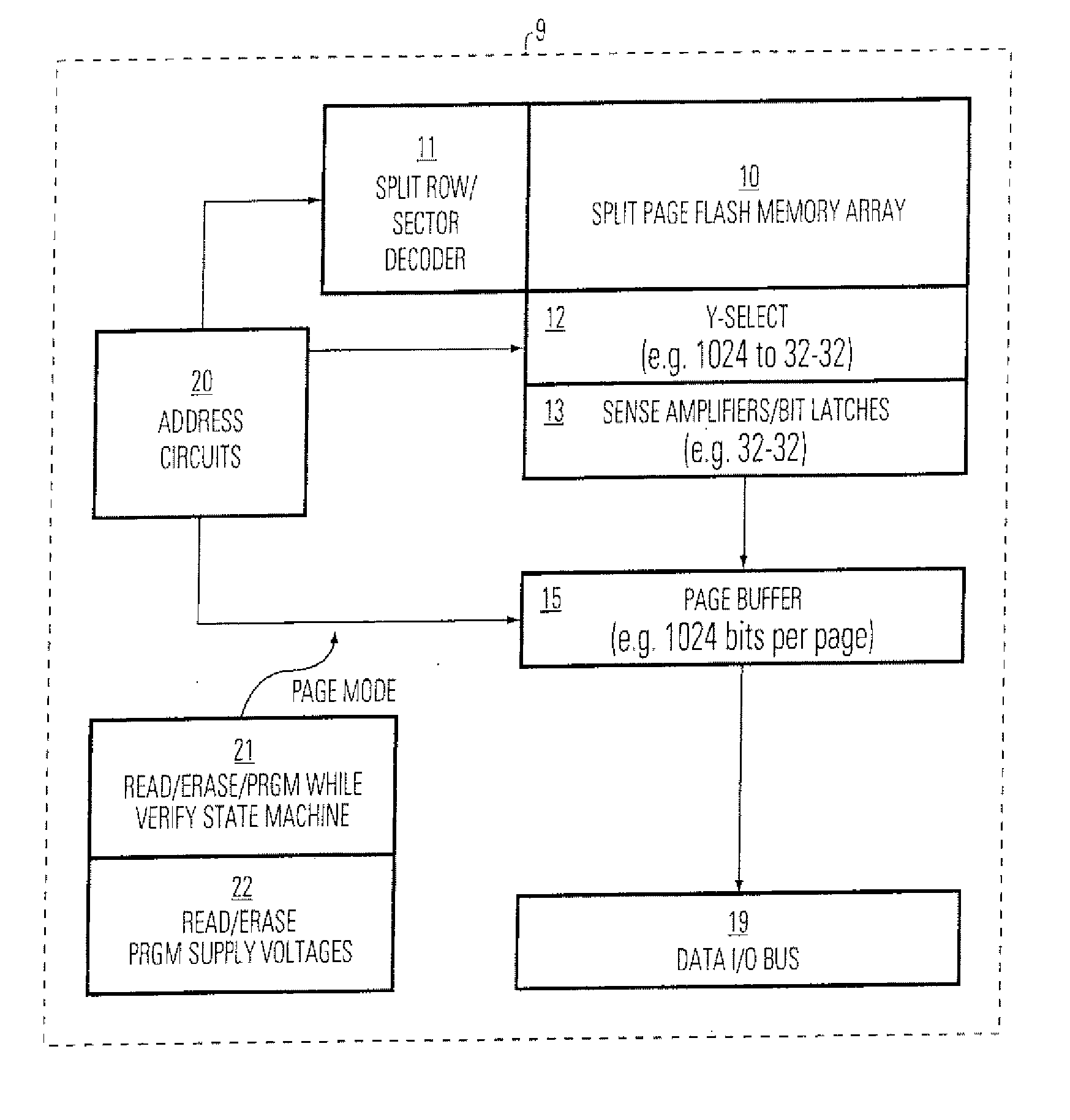
[0028]FIG. 1 is a simplified block diagram of a single chip, integrated circuit memory device 9 supporting page mode operations and program while verify operations. The memory device 9 includes a flash memory array 10 that includes an array of memory cells typically organized into a plurality of sectors, and accessible using a plurality of bit lines, a plurality of word lines and a plurality of sector select lines. A row decoder 11 is used for accessing selected word lines and sectors. The plurality of word lines include pairs of word lines that are accessed in response to identical higher order address bits, as explained below. A Y-select column decoder 12 is used for accessing selected bit lines. A plurality of sense amplifiers 13, or other sensing circuitry, is coupled to data lines from the output of the column decoder 12, and arranged to sense two chunks of data in...


PUM


Abstract

A page mode program sequence is described that includes first and second bias applying cycles. In the first cycle, a program bias is applied to a first part of a page of memory cells, while a program verify bias is applied to, and data is sensed from, a second part of the page. In this manner, a first part of the page is programmed, while a second part of the page is verified. This operation is followed by a second bias applying cycle, in which a program bias is applied to the second part of the page, while a program verify bias is applied to, and data is sensed from, the first part of the page.

Description

BACKGROUND OF THE INVENTION [0001] 1. Field of the Invention [0002] The present invention relates to nonvolatile memory devices, including flash memory and page mode flash memory, which include program and program verify operations. [0003] 2. Description of Related Art [0004] Nonvolatile memory devices typically include a memory array comprising memory cells that maintain their data even when electrical power has been removed from the device. There are a variety of types of nonvolatile memory devices. One type includes so-called “read only memory,” like mask ROM in which the data is stored in the memory cell by implanting impurities in the channel region of MOS transistors. The data stored in mask ROM devices, and other nonvolatile read only memory devices, cannot be changed in the field. Another type of nonvolatile memory device includes electrically erasable and programmable memory cells, such as flash memory. The data stored in flash memory cells, and other nonvolatile electrical...

Claims


Application Information

Patent Timeline
Patent Type & Authority Applications(United States)
IPC IPC(8): G11C11/34
CPCG11C16/3468
Inventor HO, WEN CHIAOSHIH, YI CHUNCHANG, CHIN-HUNGHUNG, CHUN-HSIUNG
Owner MACRONIX INT CO LTD
Why Eureka
Try Eureka