Defect detecting device, image sensor device, image sensor module, image processing device, digital image quality tester, and defect detecting method

Inactive Publication Date: 2007-03-29
SHARP KK
View PDF15 Cites 42 Cited by
  • Summary
  • Abstract
  • Description
  • Claims
  • Application Information

AI Technical Summary

Benefits of technology

[0036] The present invention has an objective to provide a defect detecting device having small circuitry, but still being capable of quickly determining whether there is a defective region in a digital image, and also

Problems solved by technology

Image data is never uniform across the screen even on a high quality image sensor device due to shading and noise.
Especially, when an image sensor image has a point defect, spot defect, or stain defect, the pixel data changes in a complex manner in accordance with that particular defect.
This could be a cause for different inspection standards among inspection personnel, inconsistent inspection results due to the physical condition of the inspector at the time of inspection, and difficulty in quantification of spot and stain defects.
This is due to relatively poor sensitivity of pixels along the edges of the image in comparison to the sensitivity of the pixels at the center.
For example, filtering on 3×3 pixels does not work with pixels along the edges of the image, since those pixels do not have a complete set of adjacent pixels.
With growing numbers of pixels in an image sensor image, the filtering steps and the identification number allocating step, required to enhance spot defects and stain defects in the

Method used


Image

  • Defect detecting device, image sensor device, image sensor module, image processing device, digital image quality tester, and defect detecting method
  • Defect detecting device, image sensor device, image sensor module, image processing device, digital image quality tester, and defect detecting method
  • Defect detecting device, image sensor device, image sensor module, image processing device, digital image quality tester, and defect detecting method

Examples


Embodiment Construction

1. Device Basic Structure

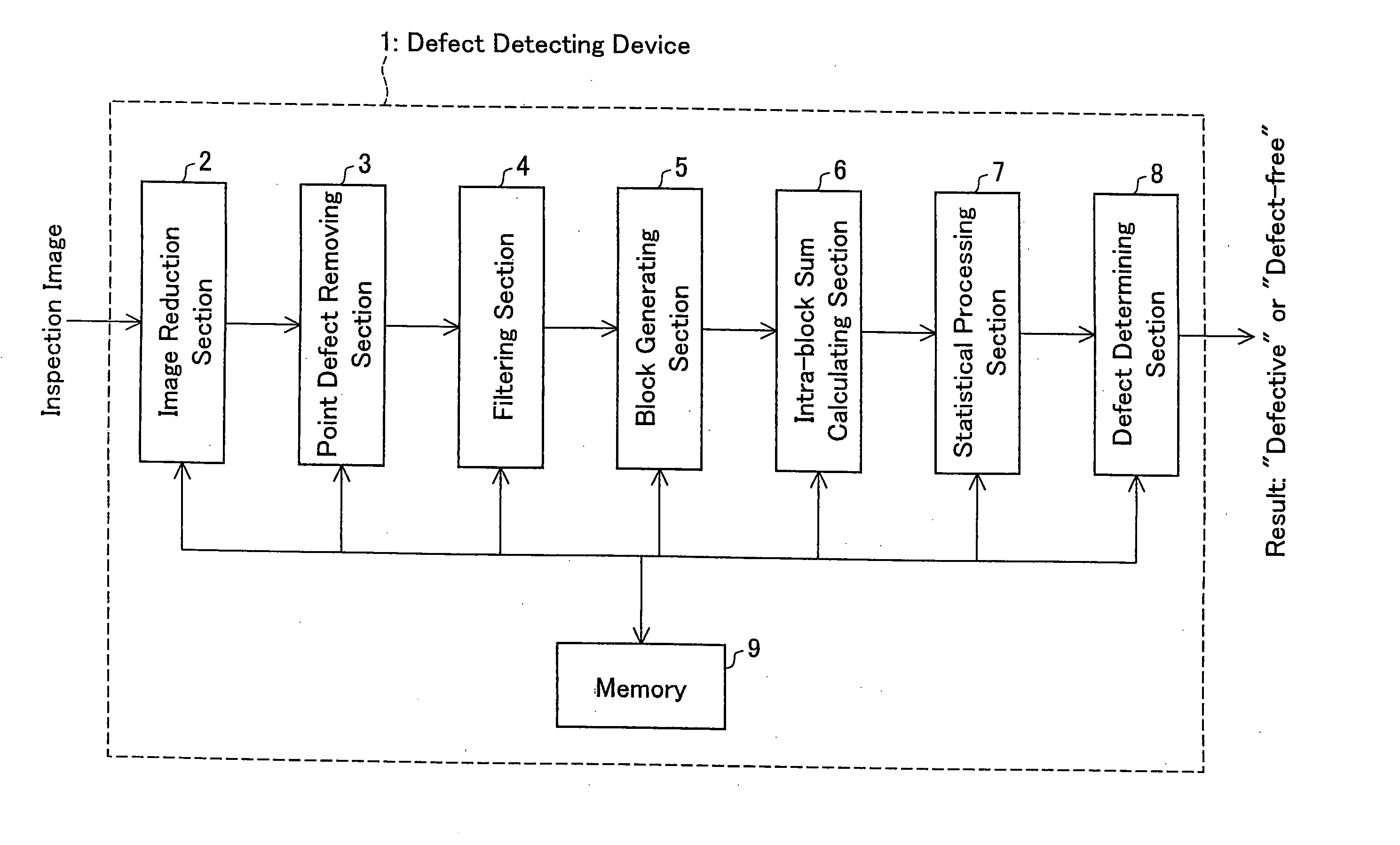
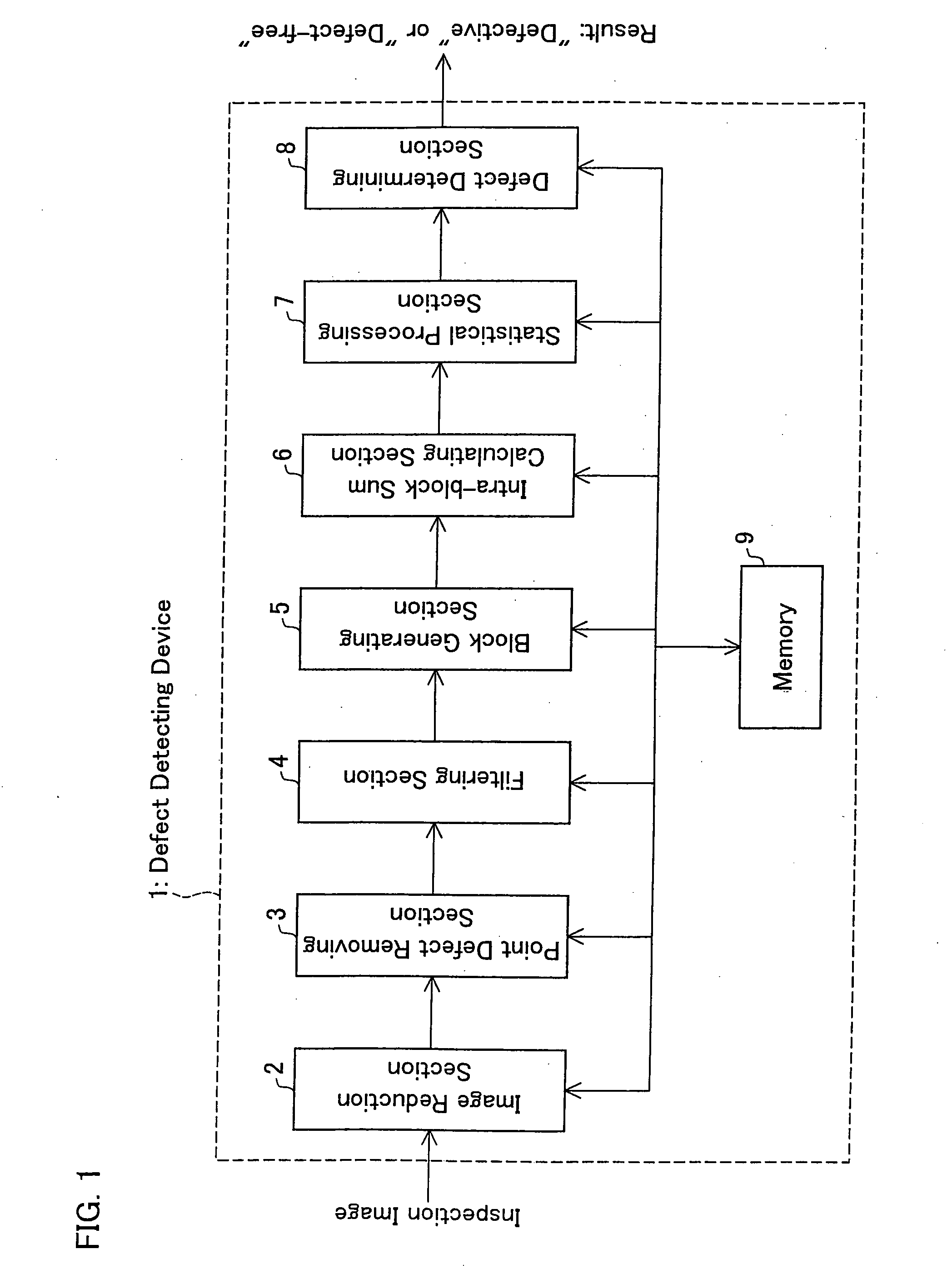
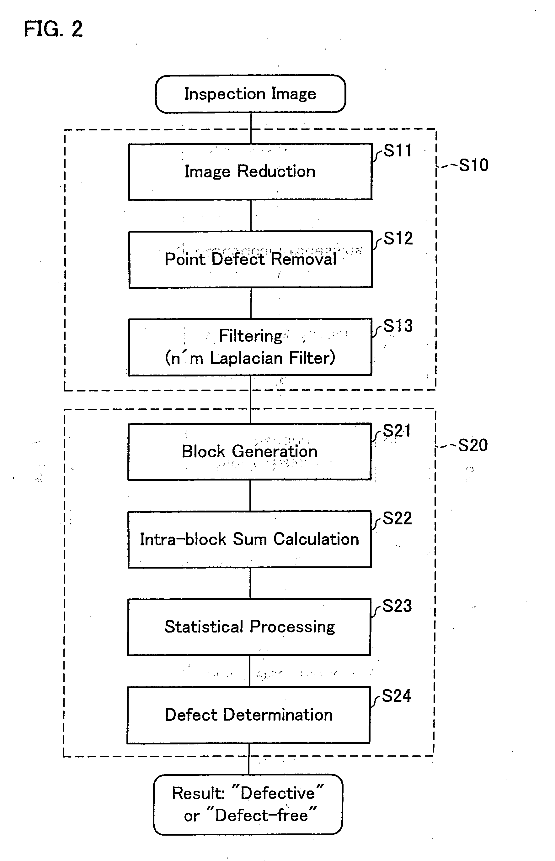
[0082] An embodiment of the defect detecting device of the present invention will be described in reference to FIG. 1. A defect detecting device 1 of the present embodiment, as shown in FIG. 1, includes an image reduction section (image reduction means) 2, a point defect removing section (point defect removing means) 3, a filtering section (filtering means) 4, a block generating section (block generating means) 5, an intra-block sum calculating section (intra-block sum calculating means) 6, a statistical processing section (defective region presence determining means) 7, a defect determining section (defective region presence determining means) 8, and a memory 9.

[0083] The image reduction section 2 reduces the inspection image in both vertical and horizontal dimensions. The downscaling reduces the data size of the inspection image and makes spot defects and stain defects in the inspection image more prominent.

[0084] The point defect removing section 3 re...


PUM


Abstract

A defect detecting device includes: a block generating section dividing an inspection image in which a defective region will be detected into a plurality of blocks; an intra-block sum calculating section calculating an intra-block sum for each of the blocks generated by the block generating section, the intra-block sum being a sum of pixel data for pixels in that block; and a statistical processing section and a defect determining section determining whether there exists a defective region by determining through statistical processing whether the intra-block sums have an outlier. Accordingly, the device determines whether there is a defective region in a digital image quickly and using small circuitry.

Description

[0001] This nonprovisional application claims priority under 35 U.S.C. § 119(a) on Patent Application No. 2005-280888 filed in Japan on Sep. 27, 2005, the entire contents of which are hereby incorporated by reference. FIELD OF THE INVENTION [0002] The present invention relates to a defect detecting device having small circuitry, but still being capable of quickly determining whether there is a defective region in a digital image. The invention also relates to an associated image sensor device, image sensor module, image processing device, digital image quality tester, defect detecting method, defect detecting computer program, and computer-readable storage medium. The invention enables small circuitry to quickly determine whether there is a defective region in a digital image. The invention is especially suitable for use in quality inspection of image sensor devices (there is growing demand for high quality image sensor devices). The invention is applicable not only to the inspectio...

Claims


Application Information

Patent Timeline
IPC IPC(8): G06K9/00
CPCG06T7/0004
Inventor KUCHII, TOSHIMASAICHIHARA, HIDEYUKI
Owner SHARP KK
Why Eureka
Try Eureka