

Substrate processing apparatus
a processing apparatus and substrate technology, applied in the direction of photomechanical apparatus, instruments, photosensitive materials, etc., can solve the problem of not being able to make a resist pattern finer than
- Summary
- Abstract
- Description
- Claims
- Application Information
AI Technical Summary
Benefits of technology
Problems solved by technology
Method used
Image

Examples
Embodiment Construction
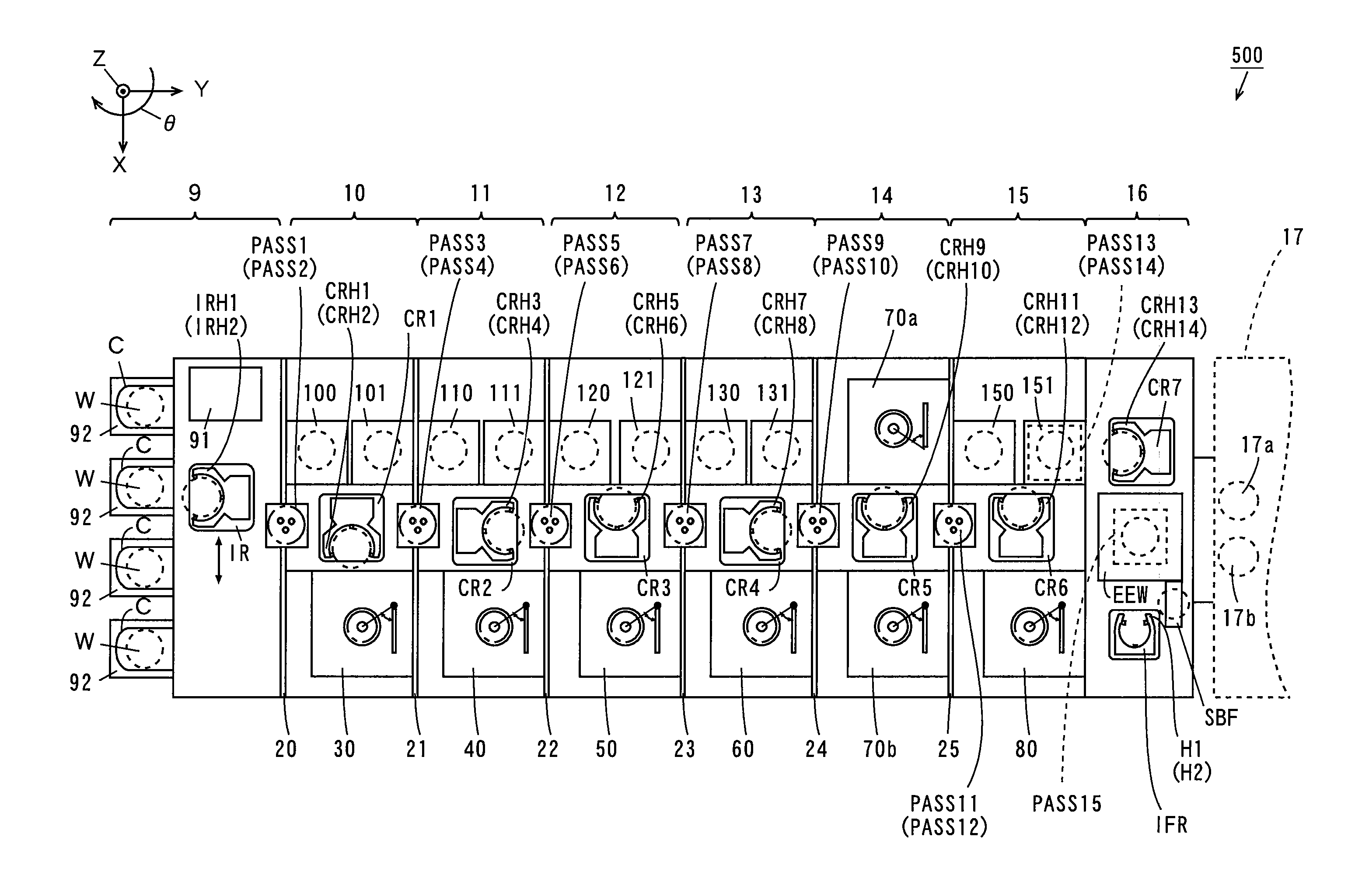
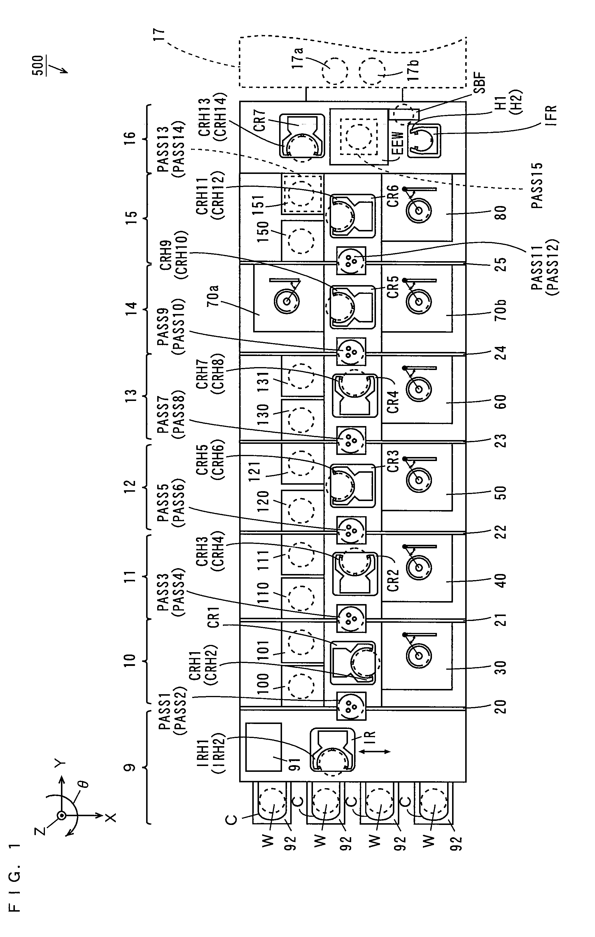
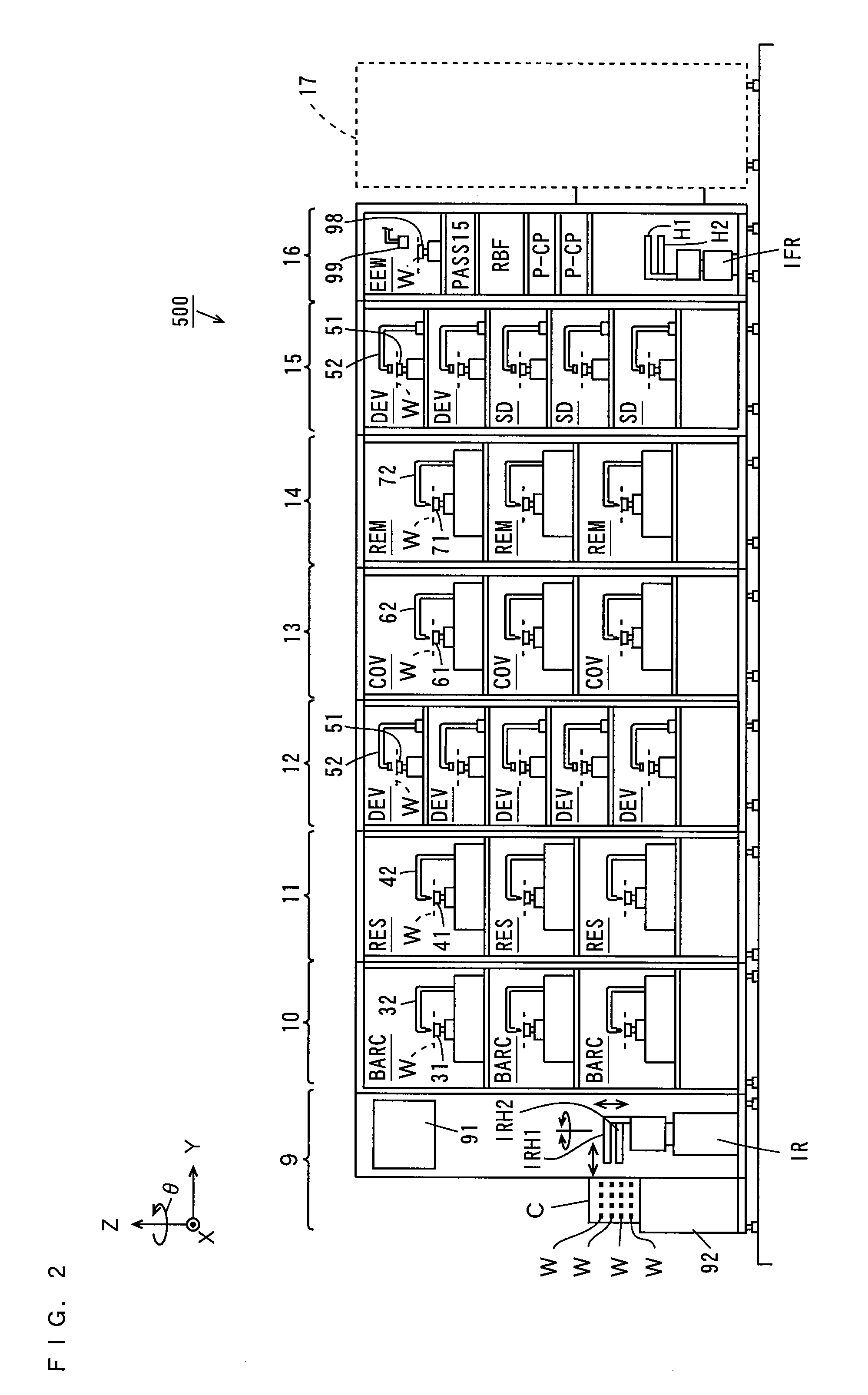
[0059] Substrate processing apparatuses according to the embodiment of the invention will be described with reference to the drawings.
[0060] A substrate as used in the description below includes a semiconductor substrate, a substrate for a liquid crystal display, a substrate for a plasma display, a glass substrate for a photomask, a substrate for an optical disk, a substrate for a magnetic disk, a substrate for a magneto-optical disk, and a substrate for a photomask.
[0061] Furthremore, the subsequent drawings are accompanied by the arrows that indicate X, Y, and Z directions perpendicular to one another for clarification of positions. The X and Y directions are perpendicular to each other in a horizontal plane, and the Z direction corresponds to the vertical direction. In each of the directions, the direction at which an arrow points is defined as + direction, and the opposite direction is defined as − direction. The rotation direction centered around the Z direction is defined as...
PUM
 Abstract
Description
Claims
Application Information