Semiconductive coating and application process for shielded elastomeric electrical cable accessories

a technology of elastomeric insulating dielectrics and semi-conductive coatings, which is applied in the manufacture of non-conductive materials with dispersed conductive materials, cable/conductor devices, woodworking apparatuses, etc., can solve the problem that the chemical bonding between an elastomeric semi-conductive coating and an elastomeric insulating dielectric cannot be satisfactorily achieved, and the application of secondary coatings to irregular interior surfaces is difficult to achieve effectively and cost. problem problem

Inactive Publication Date: 2007-04-05
THOMAS & BETTS INT INC
View PDF16 Cites 2 Cited by
  • Summary
  • Abstract
  • Description
  • Claims
  • Application Information

AI Technical Summary

Benefits of technology

[0014] The present invention will allow coating thickness as low as 0.0005 inches and requires only one molding operation. In addition, due to the method of applying the coating, there is no need for secondary operations of trimming flash or cleaning. The present invention also results in significant reduction of raw material usage without any adverse effects on the physical characteristics, especially the modulus or stiffness of the final product. The invention allows the transfer of coating from an intermediate exterior surface to any interior surface, regardless of the geometry or surface irregularity. The invention results in the transfer and subsequent cross-linking of the semiconductive coating simultaneously with the cure of the elastomeric insulating dielectric. Furthermore, it is contemplated that the formulated semiconductive coating may be made without a catalyst, thereby rendering the shelf life of the final product indefinite.

Problems solved by technology

The thicker pre-molded semiconductive components may impart undesirable physical characteristics to the final product.
The application of the secondary coating to irregular interior surfaces is very difficult to achieve effectively and is costly to apply.
Chemical cross-linking (chemical bonding) between an elastomeric semiconductive coating and an elastomeric insulating dielectric cannot be satisfactorily achieved unless the coating is subsequently cured or vulcanized by using heat and / or pressure during a secondary operation.
The shelf life of these components is limited in that the coatings are reactive systems containing catalysts.

Method used


Image

  • Semiconductive coating and application process for shielded elastomeric electrical cable accessories
  • Semiconductive coating and application process for shielded elastomeric electrical cable accessories
  • Semiconductive coating and application process for shielded elastomeric electrical cable accessories

Examples


Embodiment Construction

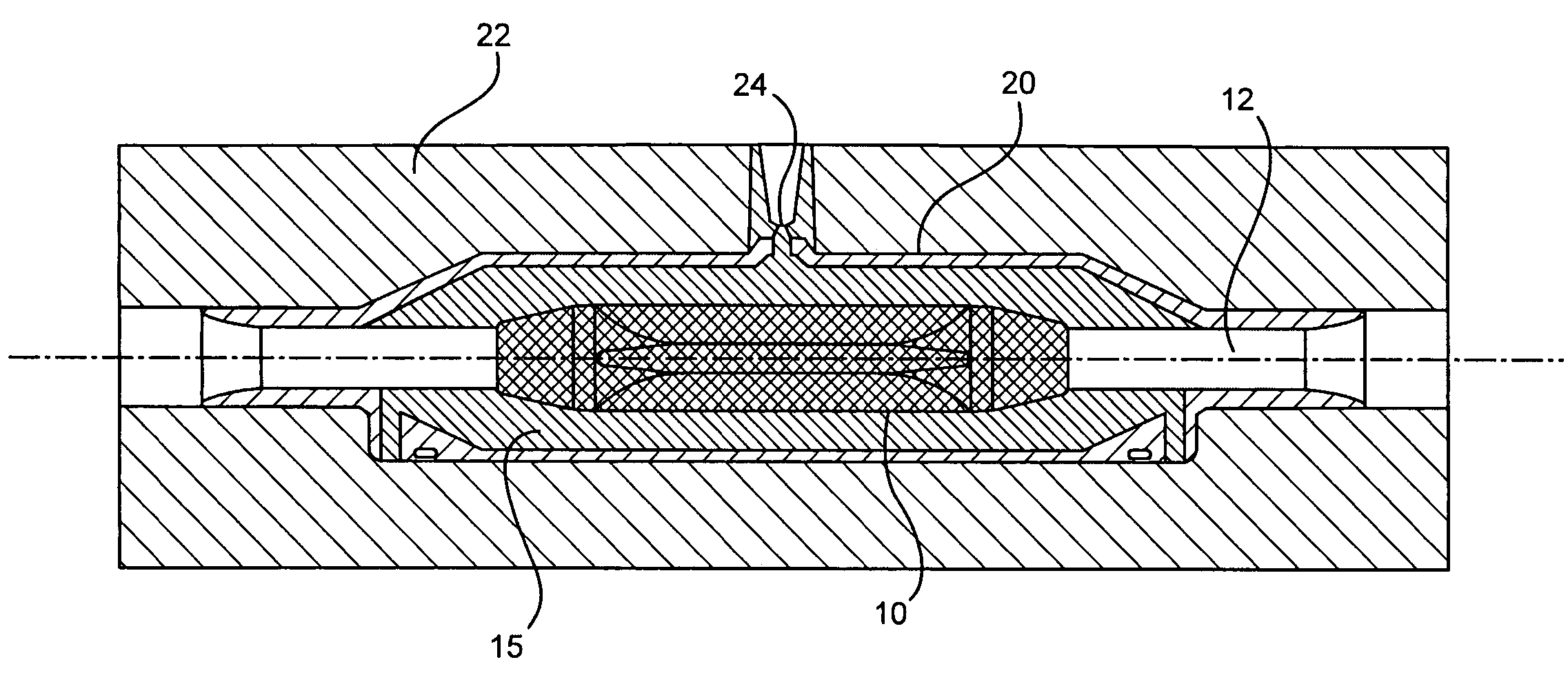
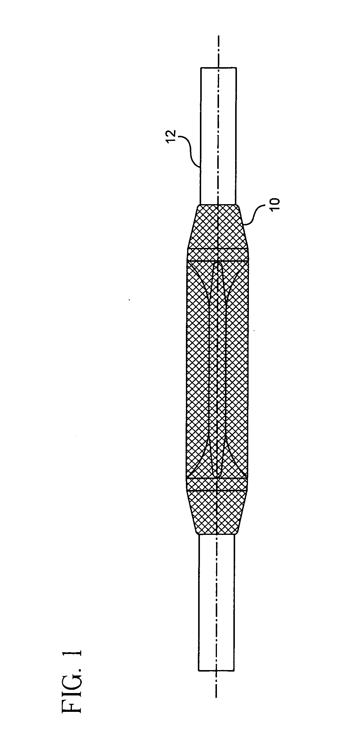
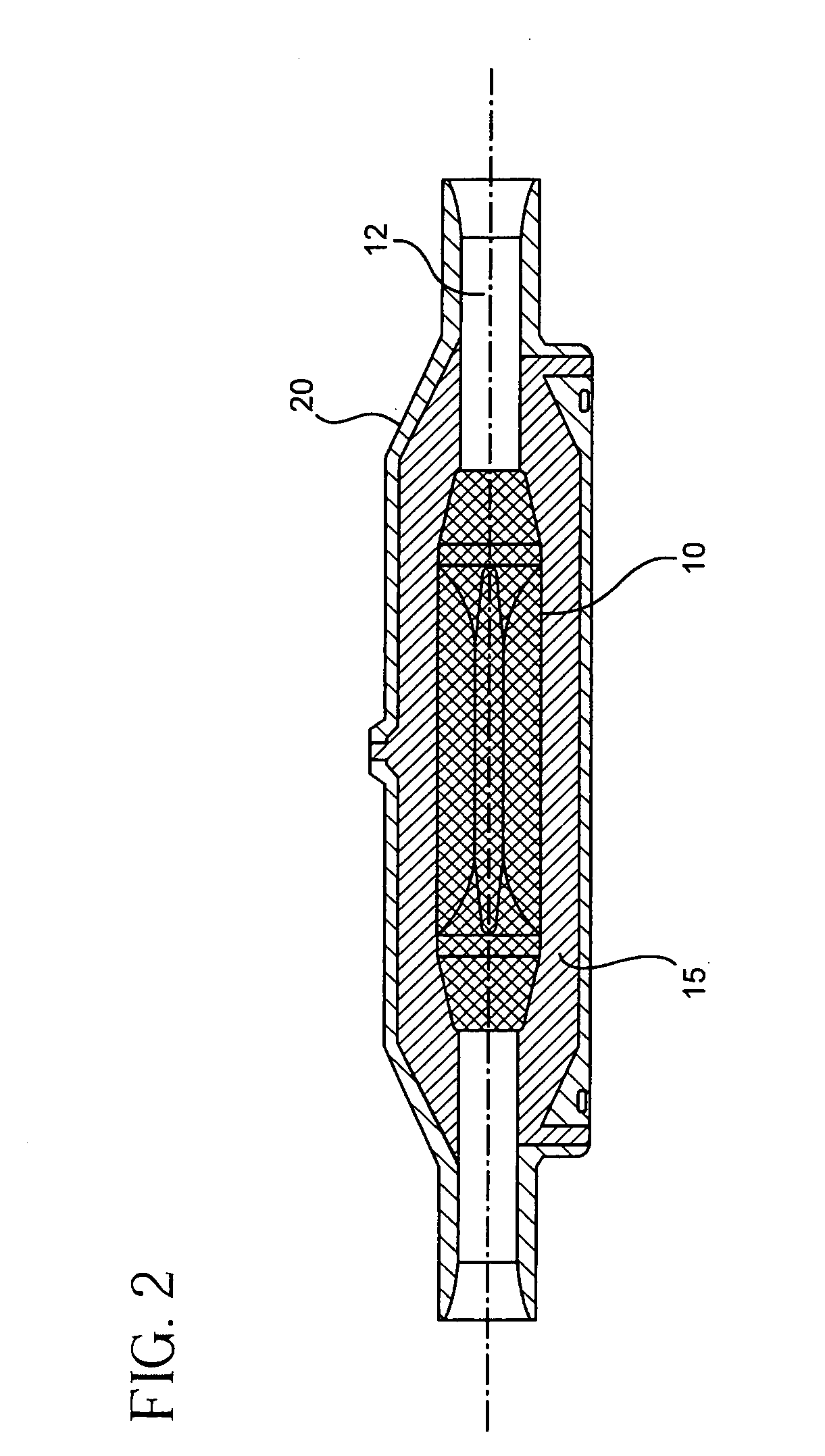
[0018] The present invention provides a method for manufacturing a semiconductive shield capable of providing geometric electrical stress control and / or shielding to medium to high voltage electrical cable accessories. The process of the present invention includes the transfer of a conventionally applied elastomeric semiconductive coating from an intermediate substrate to an elastomeric insulating dielectric during cure of the coating and insulating dielectric.

[0019] The present invention includes an elastomeric semiconductive coating process by which an elastomeric semiconductive coating is transferred from an intermediate substrate to an elastomeric insulating dielectric during the cure of the coating and elastomeric insulating dielectric. The formulated elastomeric semiconductive coating may include, for example, an EPDM elastomer. However, the formulated coatings may also be based on silicone (VMQ) and other elastomeric polymers.

[0020] The elastomeric semiconductive coating us...


PUM

PropertyMeasurementUnit
thickaaaaaaaaaa
thicknessaaaaaaaaaa
semiconductiveaaaaaaaaaa

Abstract

A method is provided for manufacturing a semiconductive insulating shield for an electrical cable accessory. The method includes providing a substrate having a desired contour in relation to the electrical cable accessory. The substrate is then coated with an elastomeric semiconductive material to form a coated substrate. An elastomeric insulating dielectric material is then molded around the coated substrate, and the elastomeric semiconductive material and elastomeric insulating dielectric material are cured by applying heat and pressure sufficient to transfer the elastomeric semiconductive material to the elastomeric insulating dielectric material by chemical bonding.

Description

CROSS-REFERENCE TO RELATED APPLICATIONS [0001] This application claims priority to application Ser. No. 10 / 339,054, filed Jan. 9, 2003 which is hereby incorporated by reference.FIELD OF THE INVENTION [0002] The present invention relates to shielded electrical cable accessories. More particularly, the present invention relates to a method for manufacturing a semiconductive shield useful for providing geometric electrical stress control and shielding to medium and high voltage electrical cable accessories. BACKGROUND OF THE INVENTION [0003] Termination or connection of high or medium voltage electrical cables in the field requires electrical shielding or stress control. Geometric electrical stress control and / or shielding of elastomeric cable accessories may be generally accomplished by one of the two following methods. [0004] In one method, an elastomeric semiconductive geometric stress control insert is pre-molded in one manufacturing operation. The insert is subsequently bonded to ...

Claims


Application Information

Patent Timeline
Patent Type & Authority Applications(United States)
IPC IPC(8): B29C43/02B28B3/02H01B11/06B05D5/12H01B9/02H01B3/28H01B3/44H02G1/14H02G15/08H02G15/103H02G15/184
CPCH01B3/28H01B3/441H02G1/145H02G15/103H02G15/184B29C45/14H01B13/22H01B1/14
Inventor BOLCAR, JOHN PAUL
Owner THOMAS & BETTS INT INC
Why Eureka
Try Eureka