Semiconductor memory

Inactive Publication Date: 2007-04-12
SOCIONEXT INC
View PDF2 Cites 27 Cited by
  • Summary
  • Abstract
  • Description
  • Claims
  • Application Information

AI Technical Summary

Benefits of technology

[0008] It is an object of the present invention to improve a write margin of a memory cell, in particular, to improve a write margin of a memory cell without any increase in circuit scale.
[0009] According to one embodiment of the present invention, each of memory cells has a pair of inverters whose inputs and outputs are connected to each other, and holds complementary data respectively in storage nodes which are the outputs of the inverters. In a write operation during which the complementary data are written to the storage nodes respectively, a power control circuit sets a power supply voltage of the inverter having the storage node to which low level is written, to be lower than a power supply voltage of the inverter having the storage node to which high level is written. This decreases power supply capability to the inverter having the storage node to which the low level is written, so that the voltage of this storage node e

Problems solved by technology

This decreases power supply capability to the inverter having the storage node to which the l

Method used


Image

  • Semiconductor memory
  • Semiconductor memory
  • Semiconductor memory

Examples


Embodiment Construction

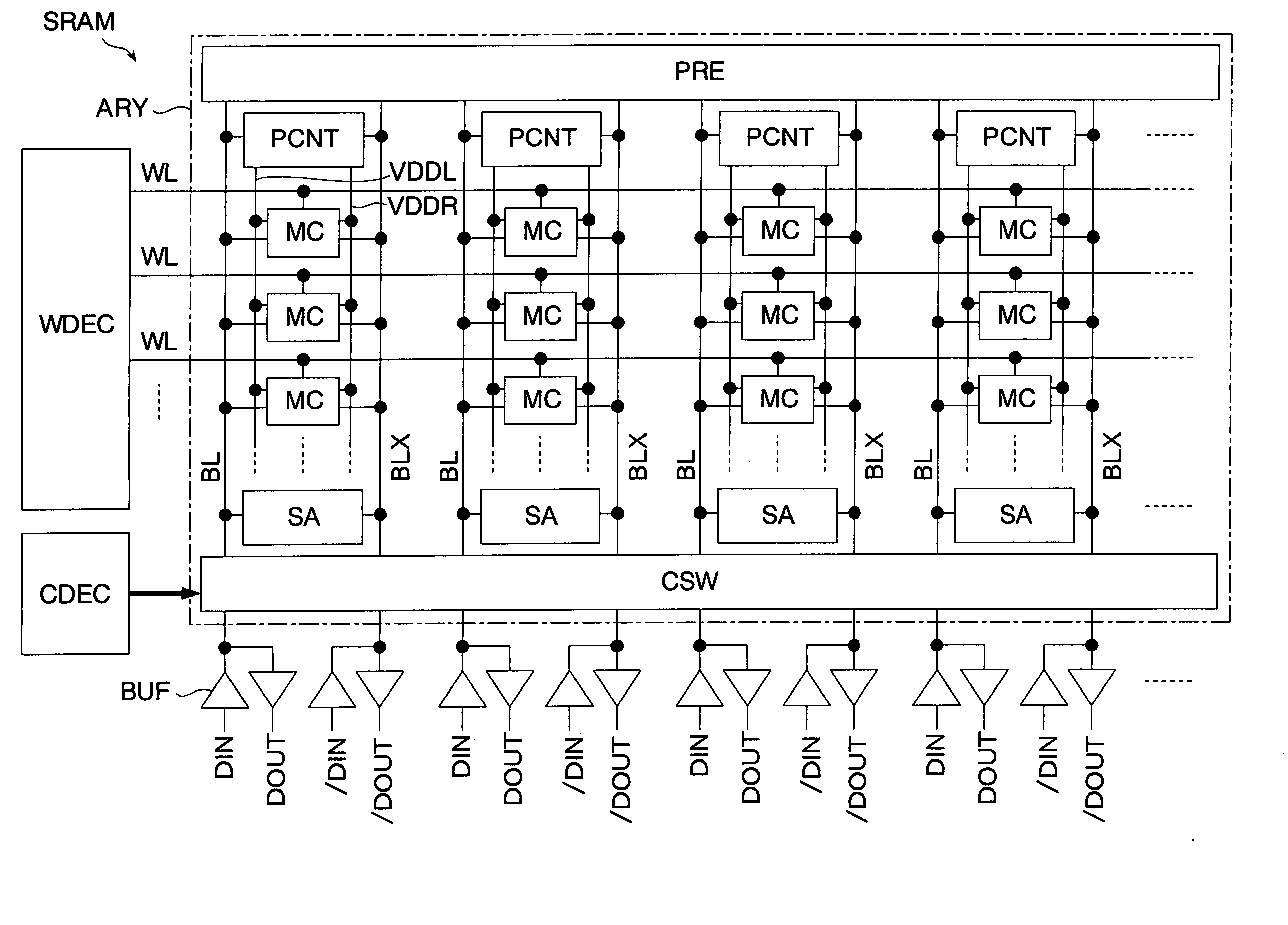
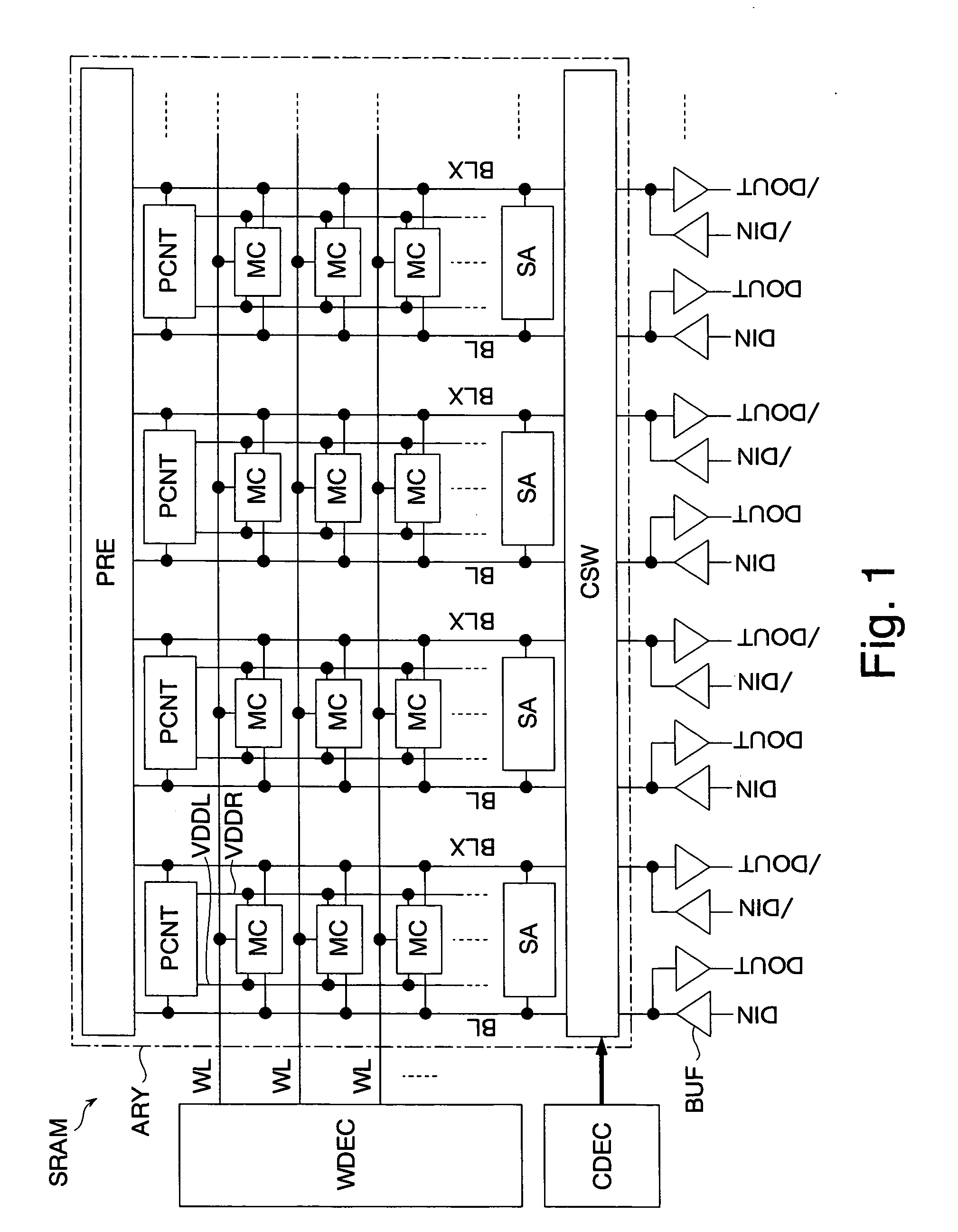
[0021] Hereinafter, embodiments of the present invention will be described, using the drawings. In the drawings, each signal line shown by the heavy line is constituted of a plurality of lines. Further, part of blocks to which the heavy line is connected is constituted of a plurality of circuits. Each signal line through which a signal is transmitted is denoted by the same reference numeral as that of the signal name. Each signal starting with “ / ” indicates negative logic. Each signal ending with “X” indicates negative logic.

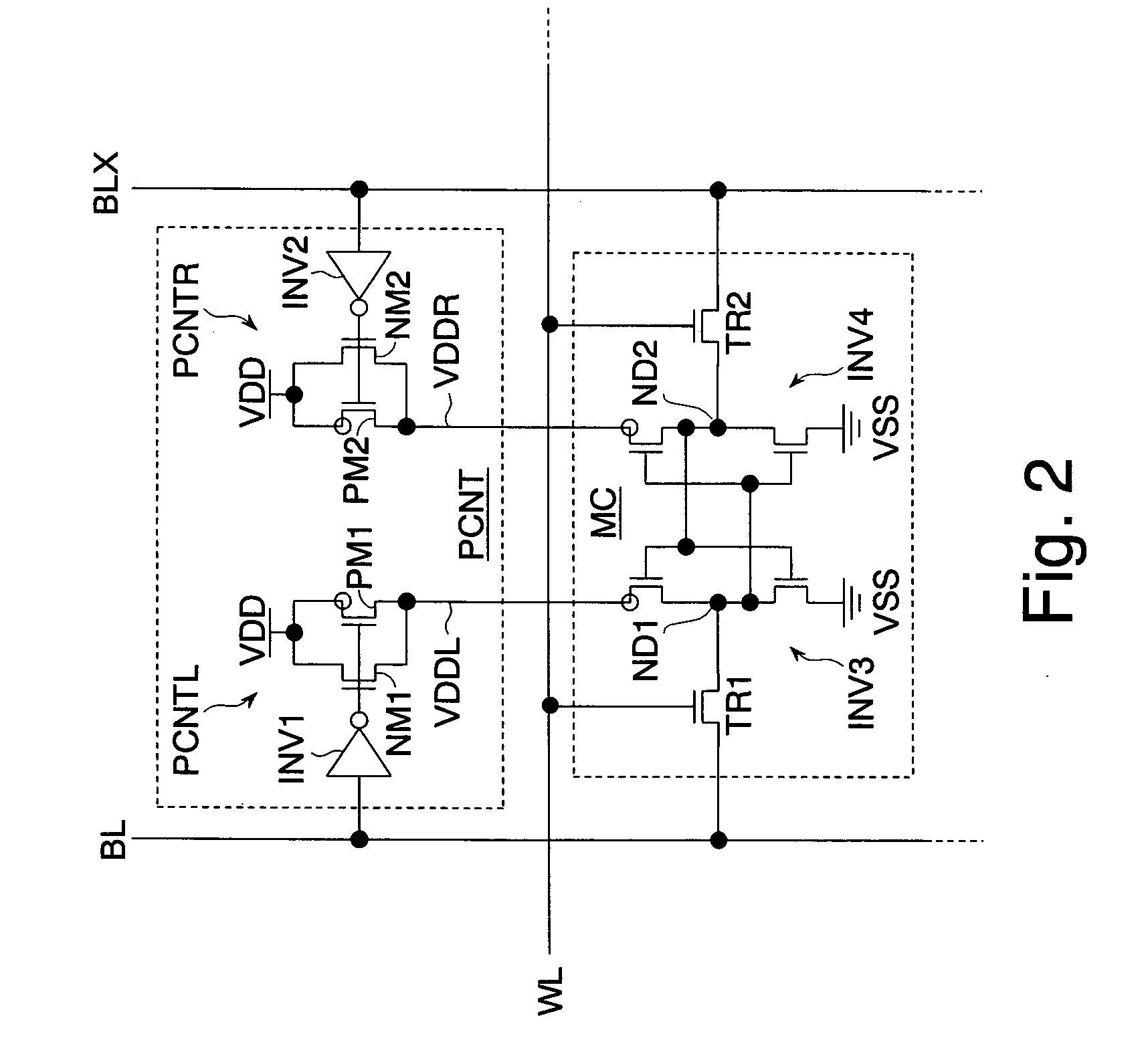
[0022]FIG. 1 shows a first embodiment of a semiconductor memory of the present invention. This semiconductor memory is formed as a SRAM having static memory cells MC by using CMOS technology. The SRAM has a memory cell array ARY, a word decoder WDEC, and a column decoder CDEC. The memory cell array ARY has a precharge circuit PRE, power control circuits PCNT, memory cells MC, sense amplifiers SA, a column switch CSW, word lines WL, and complementary bit lines B...


PUM


Abstract

Each memory cell has a pair of inverters whose inputs and outputs are connected to each other and holds complementary data respectively in storage nodes which are outputs of the inverters. In a write operation during which the complementary data are written to the storage nodes respectively, the power control circuit sets a power supply voltage of the inverter having the storage node to which low level is written lower than a power supply voltage of the inverter having the storage node to which high level is written. Since power supply capability to the inverter having the storage node to which the low level is written lowers, the voltage of the storage node easily changes to the low level. That is, a write margin of a memory cell can be improved.

Description

CROSS REFERENCE TO RELATED APPLICATION [0001] This application is based upon and claims the benefit of priority from Japanese Patent Application No. 2005-297970, filed on Oct. 12, 2005, the entire contents of which are incorporated herein by reference. BACKGROUND OF THE INVENTION [0002] 1. Field of the Invention [0003] The present invention relates to a semiconductor memory constituted of memory cells having complementary storage nodes. [0004] 2. Description of the Related Art [0005] Along with miniaturization of the device structure of a semiconductor, an insulator film constituting a transistor has been going thinner. Accordingly, reliability of the transistor has been on the decrease. A power supply voltage supplied to a semiconductor integrated circuit has been lowering year by year in order to prevent the decrease in the reliability. When the power supply voltage lowers to be less different from a threshold voltage of the transistor, the transistor is not easily turned on. Acco...

Claims


Application Information

Patent Timeline
IPC IPC(8): G11C5/14
CPCG11C11/412G11C11/419
Inventor MAKI, YASUHIKOSHIMOSAKO, KOJI
Owner SOCIONEXT INC
Why Eureka
Try Eureka