Storage unit for sram and its reading and writing methods

A technology of storage unit and bit line, which is applied in the field of SRAM storage unit and its reading and writing, to achieve the effect of improving stability, improving write tolerance and solving stability

Active Publication Date: 2019-01-29
SEMICON MFG INT (SHANGHAI) CORP
View PDF3 Cites 0 Cited by
  • Summary
  • Abstract
  • Description
  • Claims
  • Application Information

AI Technical Summary

Problems solved by technology

[0007] The embodiment of the present invention provides a storage unit for SRAM and its reading and writing method, to at least solve the technical problem of the stability of the storage unit of the existing SRAM

Method used


Image

  • Storage unit for sram and its reading and writing methods
  • Storage unit for sram and its reading and writing methods
  • Storage unit for sram and its reading and writing methods

Examples


Embodiment 1

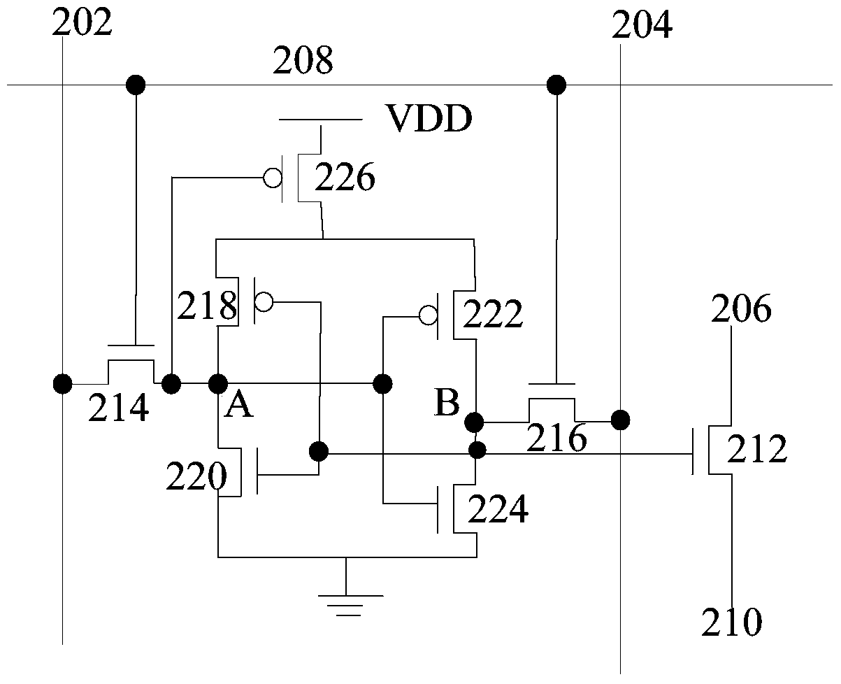
[0026] According to an embodiment of the present invention, a storage unit for SRAM is also provided, such as figure 2 As shown, the storage unit includes:

[0027] 1) The first bit line 202, the second bit line 204, the third bit line 206, the first word line 208 and the second word line 210, wherein the first word line 208 is used to control the memory cell written by the first word line The level state indicated by the bit line 202 and / or the second bit line 204, the second word line 210 is used to control the read level state from the memory cell, and the third bit line 206 is used to output the read level state;

[0028] 2) The first transistor 212 is connected between the third bit line 206 and the second word line 210 through the source and the drain, and is connected to the transistor group between the first bit line and the second bit line through the gate, and the transistor The group is used for writing the level states indicated by the first bit line and the sec...

Embodiment approach

[0033] 1) Read "1" operation: assume figure 2 Midpoint B stores data as "1", RBL is pre-charged to "1",

[0034] When RWL is currently "0", M7 is turned on, and the data "1" on point B is read through the line between M7 and point B. At this time, RBL maintains the voltage VDD state, and the signal is controlled by the amplifier SA connected to RBL. Amplify and read "1";

[0035] 2) Read "0" operation: assume figure 2 Midpoint B stores data as "0", RBL is pre-charged to "1",

[0036] When RWL is currently "0", M7 is turned on, and the data "0" on point B is read through the line between M7 and point B. At this time, RBL is discharged, and the signal is amplified and read by the amplifier SA connected to RBL. "0".

[0037] Here, when the read operation is performed, the RWL is "0" to indicate that it is at a low level, wherein the read operation can only be enabled when the RWL is set at a low level, that is, the read operation is triggered. because figure 2 The data sto...

Embodiment 2

[0064] According to an embodiment of the present invention, a method for reading a storage unit is provided for figure 2 shown in the memory cell, specifically as Figure 4 As shown, the method includes:

[0065] S402. Preset the third bit line to the first level;

[0066] S404, applying a second level to the second word line according to the first level;

[0067] S406, judging whether to read the level state stored in the storage unit according to the second level;

[0068] S408, if it is determined to read the level state stored in the memory cell, read out the stored level state from the third bit line.

[0069] Optionally, in this embodiment, the first level is a high level and the second level is a low level, or the first level is a low level and the second level is a high level.

[0070] Optionally, if it is determined to read the level state stored in the memory cell, then reading the stored level state by the third bit line includes:

[0071] S1, reading the leve...


PUM


Abstract

The invention discloses a memory cell used for a SRAM (Static Random Access Memory) and a read-write method thereof. The memory cell comprises a first bit line, a second bit line, a third bit line, a first word line, a second word line and a first transistor, wherein the first word line is used for controlling the writing of a level state indicated by the first bit line and / or the second bit line into the memory cell, the second word line is used for controlling the reading of the level state from the memory cell, and the third bit line is used for outputting the read level state; and the first transistor is connected between the third bit line and the second word line through a source electrode and a drain electrode and is connected to a transistor group between the first bit line and the second bit line through a grid electrode, and the transistor group is used for writing the level state indicated by the first bit line and the second bit line. The technical problem of poor stability of the memory cell of the traditional SRAM is solved.

Description

technical field [0001] The invention relates to the field of semiconductor manufacturing, in particular to a storage unit used for SRAM and a reading and writing method thereof. Background technique [0002] With the improvement of complementary metal oxide semiconductor (CMOS, Complementary Metal Oxide Semiconductor) process requirements, when the CMOS process size drops to 40nm or even lower, the static random access memory (SRAM, Static RAM) design requirements in CMOS also increase. However, in the existing SRAM design scheme, due to the limitation of the SRAM under the framework of the CMOS process size, how to ensure the stability of the performance of the SRAM unit has become an urgent problem to be solved. [0003] The structure of the existing 6T structure SRAM storage unit is as follows figure 1 As shown, in the existing 6T structure, a word line (WL, Word Line) is used to control the read operation or write operation, while both the read operation and the write o...

Claims


Application Information

Patent Timeline
Patent Type & Authority Patents(China)
IPC IPC(8): G11C11/419
Inventor 方伟丁艳陈双文张静潘劲东
Owner SEMICON MFG INT (SHANGHAI) CORP
Why Eureka
Try Eureka