Semiconductor integrated circuit and its producing method

A technology of integrated circuits and manufacturing methods, which is applied in semiconductor/solid-state device manufacturing, semiconductor devices, circuits, etc., and can solve the problems of storage circuit failure, no consideration, and reduction of storage unit noise margins, etc.

Inactive Publication Date: 2009-02-04
RENESAS ELECTRONICS CORP
View PDF1 Cites 0 Cited by
  • Summary
  • Abstract
  • Description
  • Claims
  • Application Information

AI Technical Summary

Problems solved by technology

However, when setting threshold voltages of logic circuits, etc., and memory circuits in the same step, considering only factors such as ease of manufacture and the like, regardless of the apparent tendency of logic circuits, etc., to increase speed and reduce power consumption of semiconductor integrated circuit devices, Although the operating speed of logic circuits etc. can be increased, the noise margin of memory cells in memory circuits is reduced
Research conducted by the present inventors reveals that this causes failure of the operation of the storage circuit which does not occur even with threshold voltages of the logic circuit etc. and the storage circuit set at the same step

Method used


Image

  • Semiconductor integrated circuit and its producing method
  • Semiconductor integrated circuit and its producing method
  • Semiconductor integrated circuit and its producing method

Examples


Embodiment 1

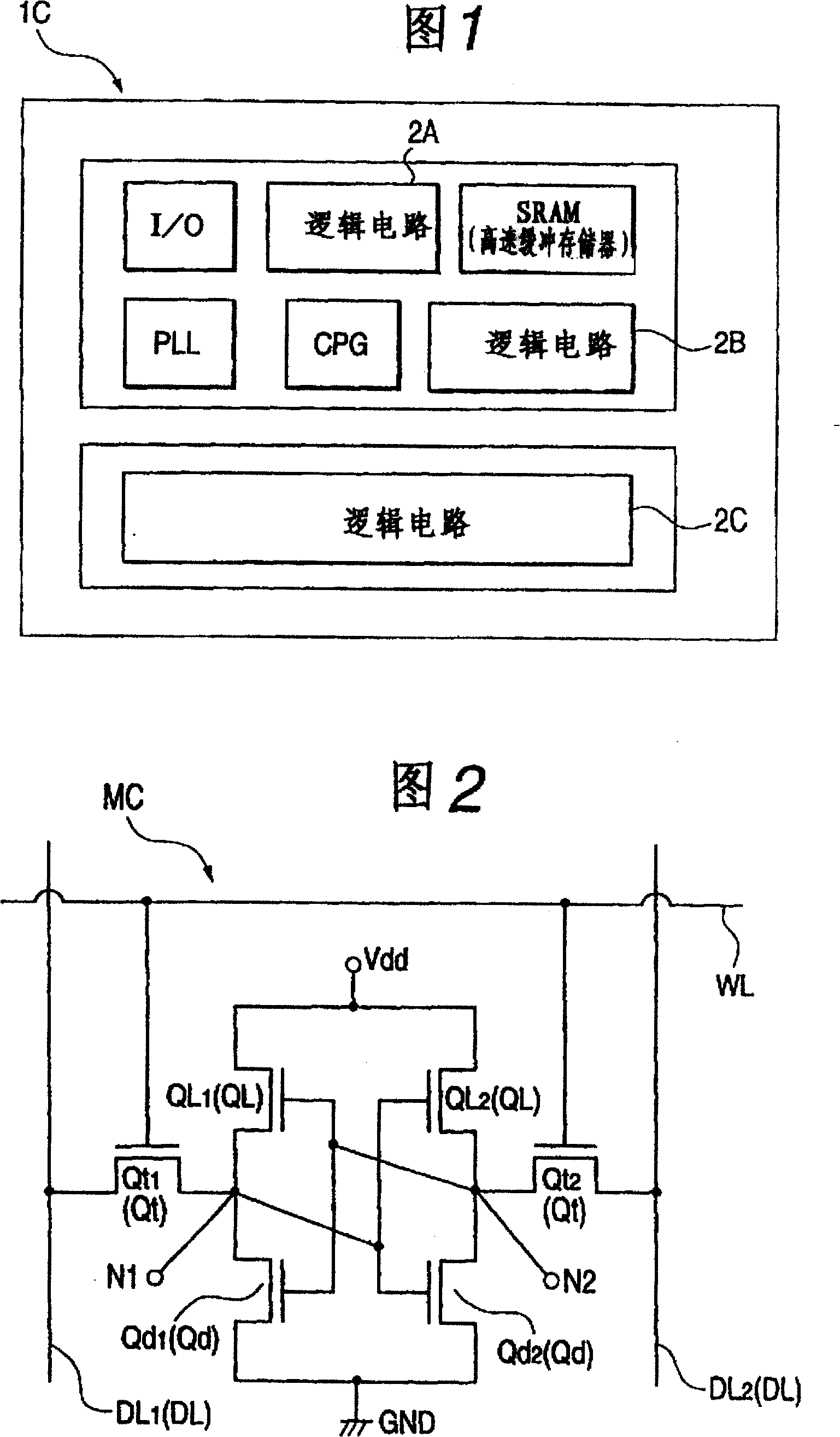
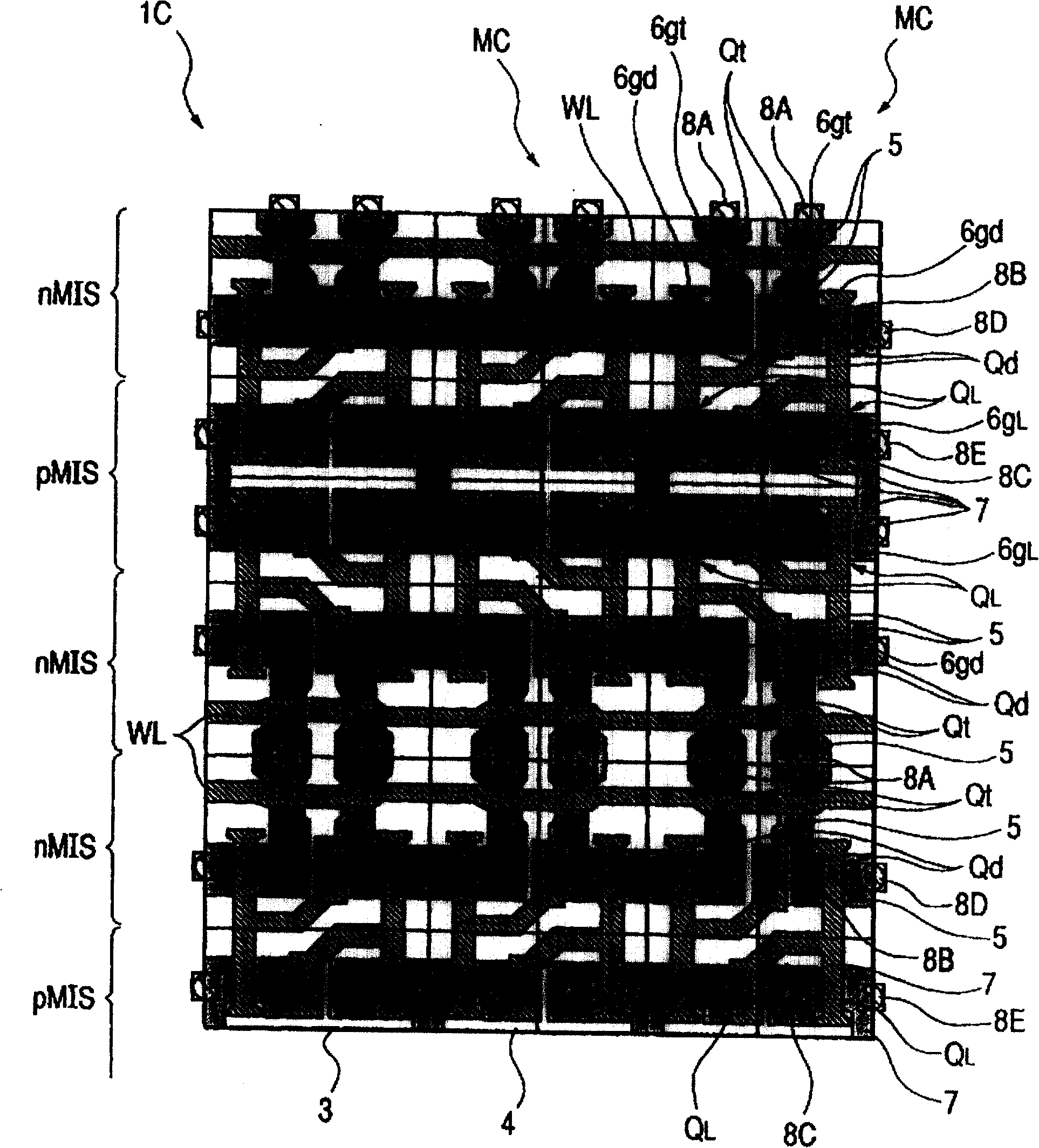
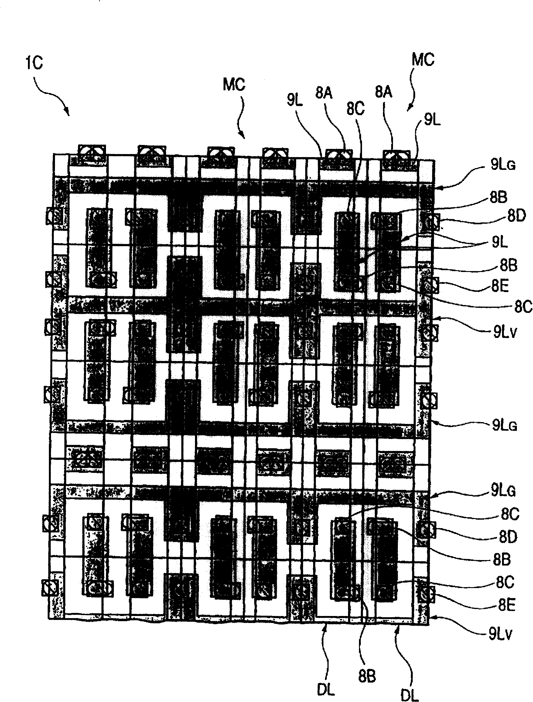
[0044] 1-4 are diagrams for explaining the structure of the semiconductor integrated circuit device of the present invention. 5-17 are cross-sectional views of main parts of the semiconductor integrated circuit device during respective manufacturing steps for explaining a method of manufacturing the semiconductor integrated circuit device in FIG. 1 . Figure 18 is a diagram explaining the effect of the current mode of carrying out the invention. Figure 19 Techniques studied by the inventors are shown to explain the effect of the current mode of carrying out the invention. FIG. 20 is a diagram explaining the effect of the current mode of implementing the present invention.

[0045] With regard to the technical principles of the pertinent field, when it is said that "threshold voltage (hereinafter expressed as Vth) is high", it means that the expected increase in Vth exceeds the increase in Vth due to differences in dimensions such as channel width. In addition, in the techni...

Embodiment 2

[0117] Figure 21 is a plan view of a main part of a semiconductor integrated circuit device of another mode for realizing the invention during manufacture.

[0118] Although said Mode 1 of implementing the invention involves the case of intentionally relatively raising the Vth of all the MISFETs constituting the memory cell of the SRAM, the present invention is not limited thereto, and the Vth of a predetermined MISFET of the memory cell of the SRAM may be relatively raised intentionally. .

[0119] Mode 2 of realizing the invention introduces this way, for example, in order to increase the Vth of the transfer MISFET relatively intentionally, it can be as Figure 21 The photoresist pattern 12A2 is formed on the semiconductor substrate 3 as shown, replacing the first process or the second process described in the mode 1 of realizing the invention. Figure 6 The photoresist pattern 12A is shown so as to expose the region where the transfer MISFET will be formed, while coverin...

Embodiment 3

[0122] Figure 22 is a plan view of a main part of a semiconductor integrated circuit device of another mode for realizing the invention during manufacture.

[0123] Mode 3 for realizing the invention is to introduce the situation where the Vth of the driving MISFET is relatively increased on purpose. In this case, it can be as follows Figure 22 Form photoresist pattern 12A3 on semiconductor substrate 3 as shown, replace said first process or second process introduced in said Mode 1 of realizing the invention (see Figure 6 ) photoresist pattern 12A, in order to expose the area where the driving MISFET will be formed, and cover other areas. Figure 22 Also demonstrated with image 3 , 6 and the same memory cell region, and various elements etc. are shown in order to clearly show the position where the photoresist pattern 12A3 is formed as described above. For the sake of clarity in the attached Figure 22 A photoresist pattern 12A3 is also drawn in . In addition, the con...


PUM


Abstract

An operational margin of a memory of a semiconductor integrated circuit device including an SRAM is improved. In order to set the Vth of driving MISFETs Qd, transfer MISFETs Qt and MISFETs for load resistance QL forming memory cells of an SRAM, relatively and intentionally higher than the Vth of predetermined MISFETs of SRAM peripheral circuits and logic circuits such as microprocessor, an impurity introduction step is introduced to set the Vth of the driving MISFETs Qd, transfer MISFETs Qt and MISFETs for load resistance, separately from an impurity introduction step for setting the Vth of the predetermined MISFETs.

Description

technical field [0001] The present invention relates to a manufacturing method of an integrated circuit device, and more particularly, to a technique effectively used for a semiconductor integrated circuit device having a static memory (SRAM; Static Random Access Memory) and a logic circuit. Background technique [0002] SRAM is a memory that uses a flip-flop circuit as a storage element. Its bistable states store information related to "1" and "0" respectively. It is characterized in that it is easy to apply, because it is different from DRAM (Dynamic Random Access Memory), It does not require a refresh operation. The trigger circuit consists of two inverting circuits. The output of one inverting circuit is electrically connected to the input of the other inverting circuit, and the output of the other inverting circuit is electrically connected to the input of the first inverting circuit. Each inverting circuit includes a drive transistor that facilitates information stor...

Claims


Application Information

Patent Timeline
Patent Type & Authority Patents(China)
IPC IPC(8): H01L27/11H01L27/10H01L21/8244H01L21/8239H01L27/105
CPCH01L27/1052H01L21/8239H01L27/105H10B99/00H10B10/00
Inventor 池田修二吉田安子儿岛雅之盐泽健治木村光行中川典夫石桥孝一郎岛崎靖久长田健一内山邦男
Owner RENESAS ELECTRONICS CORP
Why Eureka
Try Eureka