

Wiring correction method
- Summary
- Abstract
- Description
- Claims
- Application Information
AI Technical Summary
Benefits of technology
Problems solved by technology
Method used
Image

Examples
Embodiment Construction
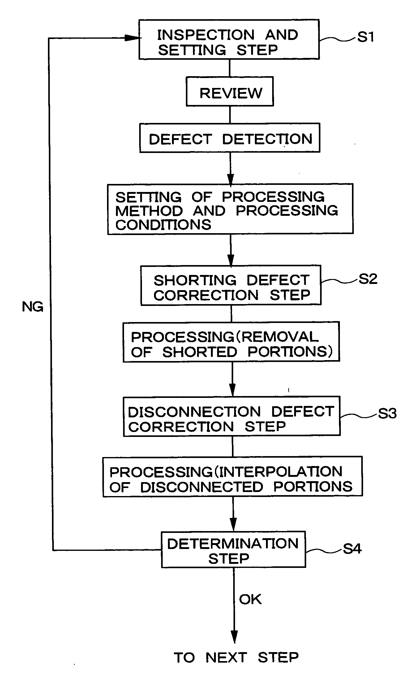
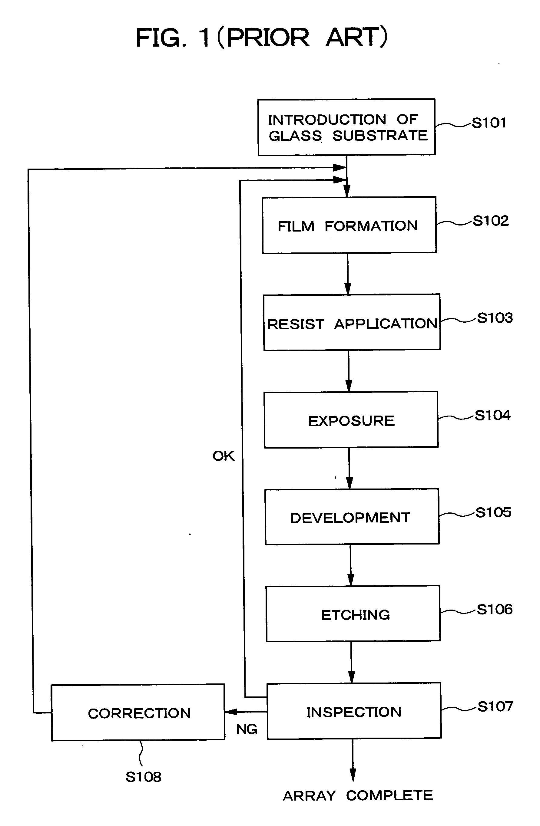
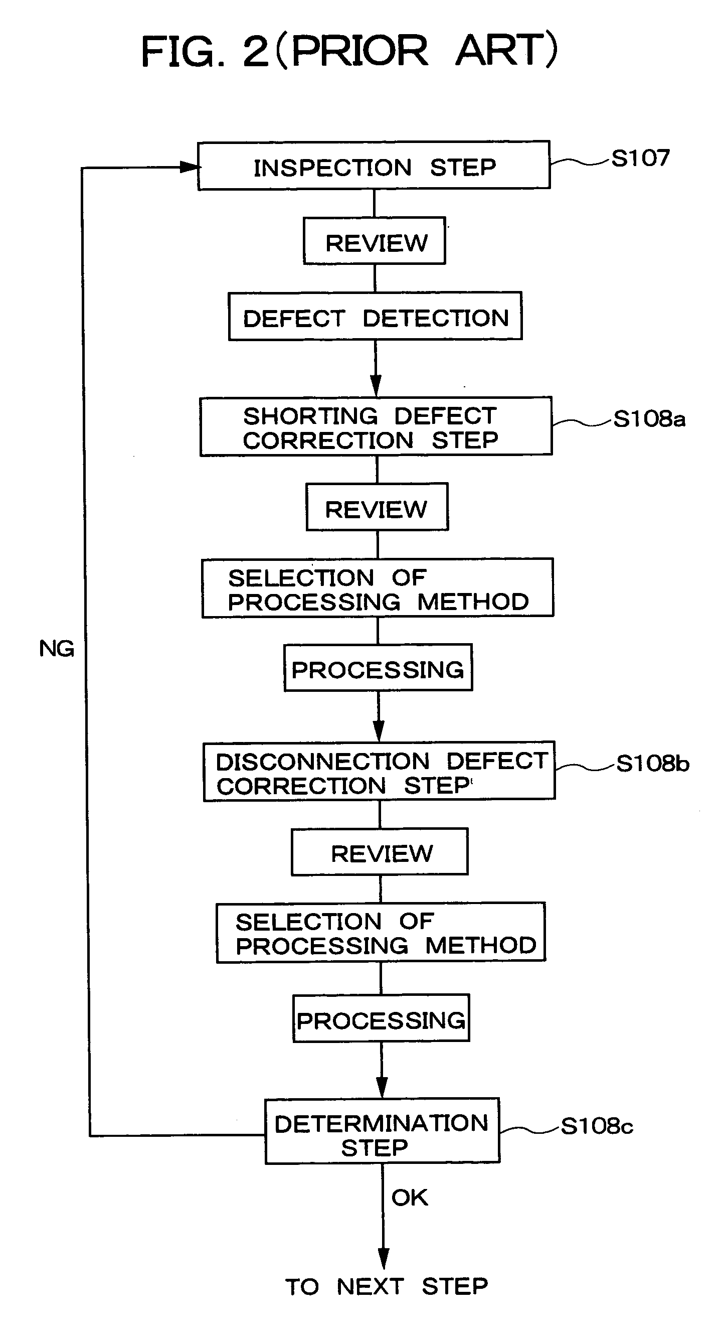
[0026] The wiring correction method according to an embodiment of the present invention is described in detail below in reference to the attached figures. The wiring correction method of the first embodiment of the present invention will be described first. FIG. 3 is a flowchart showing the wiring correction method of this embodiment. The wiring correction method of this embodiment is a method for detecting and correcting defects such as shorting defects and disconnection defects. The method is carried out after a wiring pattern has been formed in a step for manufacturing a TFT substrate for a liquid crystal display device, a step for forming the wiring of a semiconductor device, or the like. As shown in FIG. 3, the wiring correction method of this embodiment involves first detecting a wiring pattern defect, recording information regarding the defect, and then establishing the necessary settings for the subsequent correction step (step S1). Specifically, for each substrate, the pres...
PUM
 Abstract
Description
Claims
Application Information