
Initialization of flash storage via an embedded controller

a technology of flash memory and embedded controller, which is applied in the field of flash memory system initialization, can solve the problems of limiting the flexibility with which the system may be configured and initialized, adding substantial cost to the manufacture and production of the system, and conventional initialization methodologies cannot readily initialize flash memory

Active Publication Date: 2007-04-19
SANDISK TECH LLC
View PDF33 Cites 57 Cited by
  • Summary
  • Abstract
  • Description
  • Claims
  • Application Information

AI Technical Summary

Benefits of technology

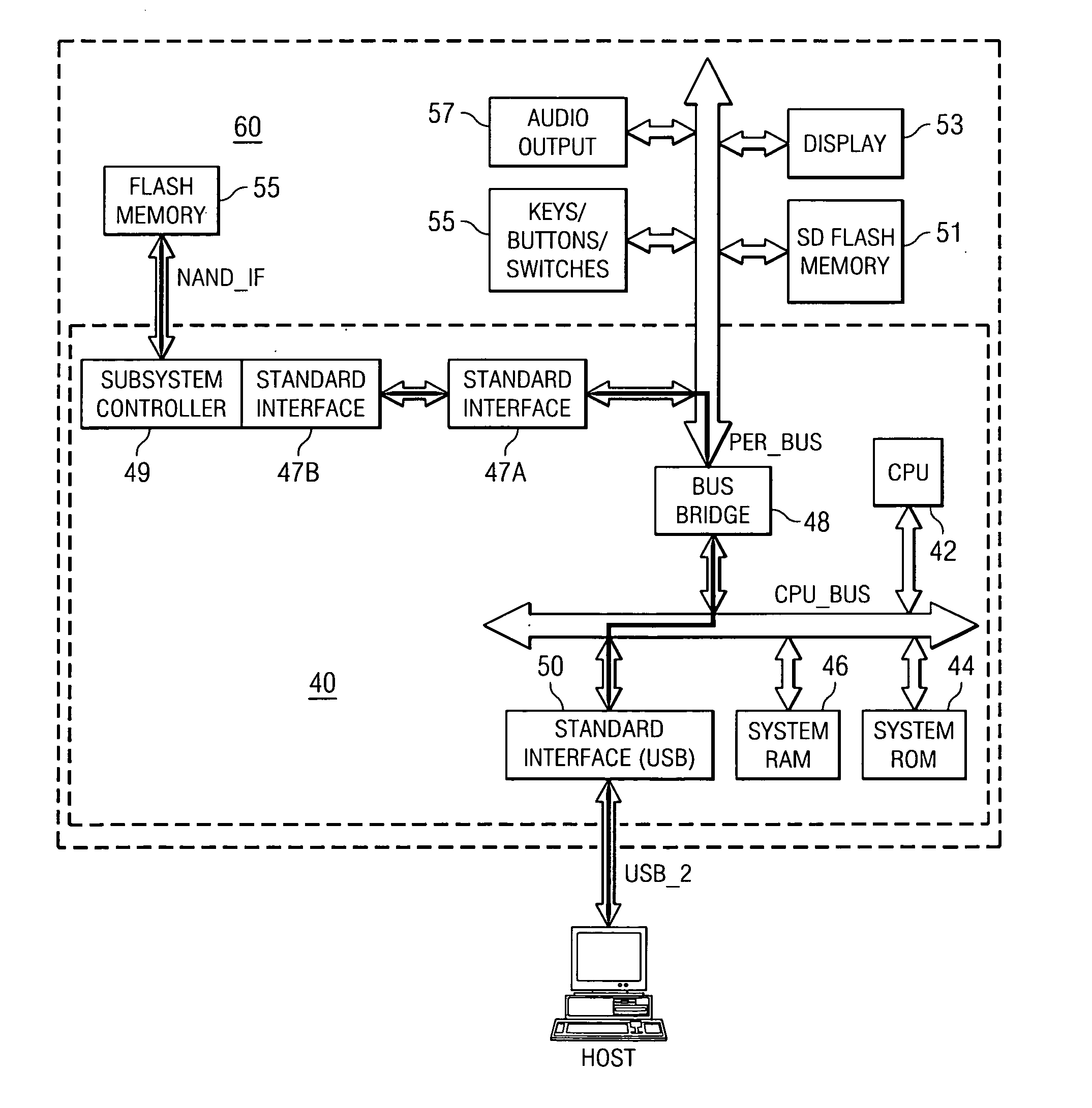
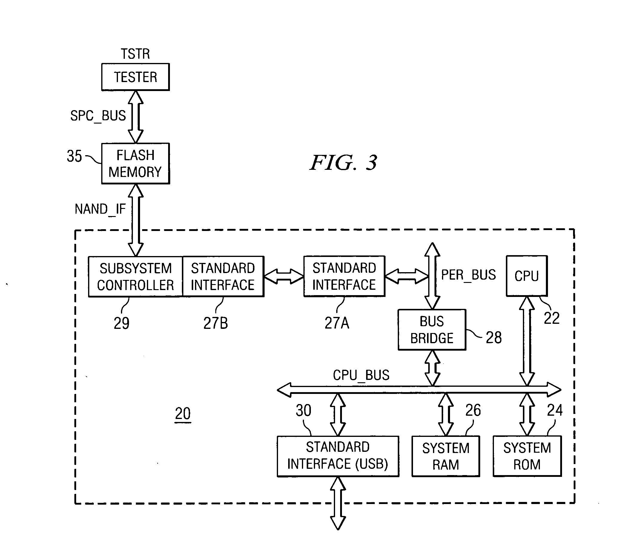
[0018] The present invention may be implemented into a system-on-a-chip (SOC) architecture in which a standard external interface of the SOC is made accessible to external test hardware. An executable initialization program that is either downloaded from the external test hardware into the system memory of the SOC or already present in system ROM will, upon execution by the CPU, open a communication channel between the external test hardware and a flash memory subsystem controller in the SOC. This communication channel enables the external test hardware to effect initialization of flash memory via the subsystem controller, preparing the flash memory for use by the SOC, loading SOC application programs onto the flash memory, and the like.

Problems solved by technology

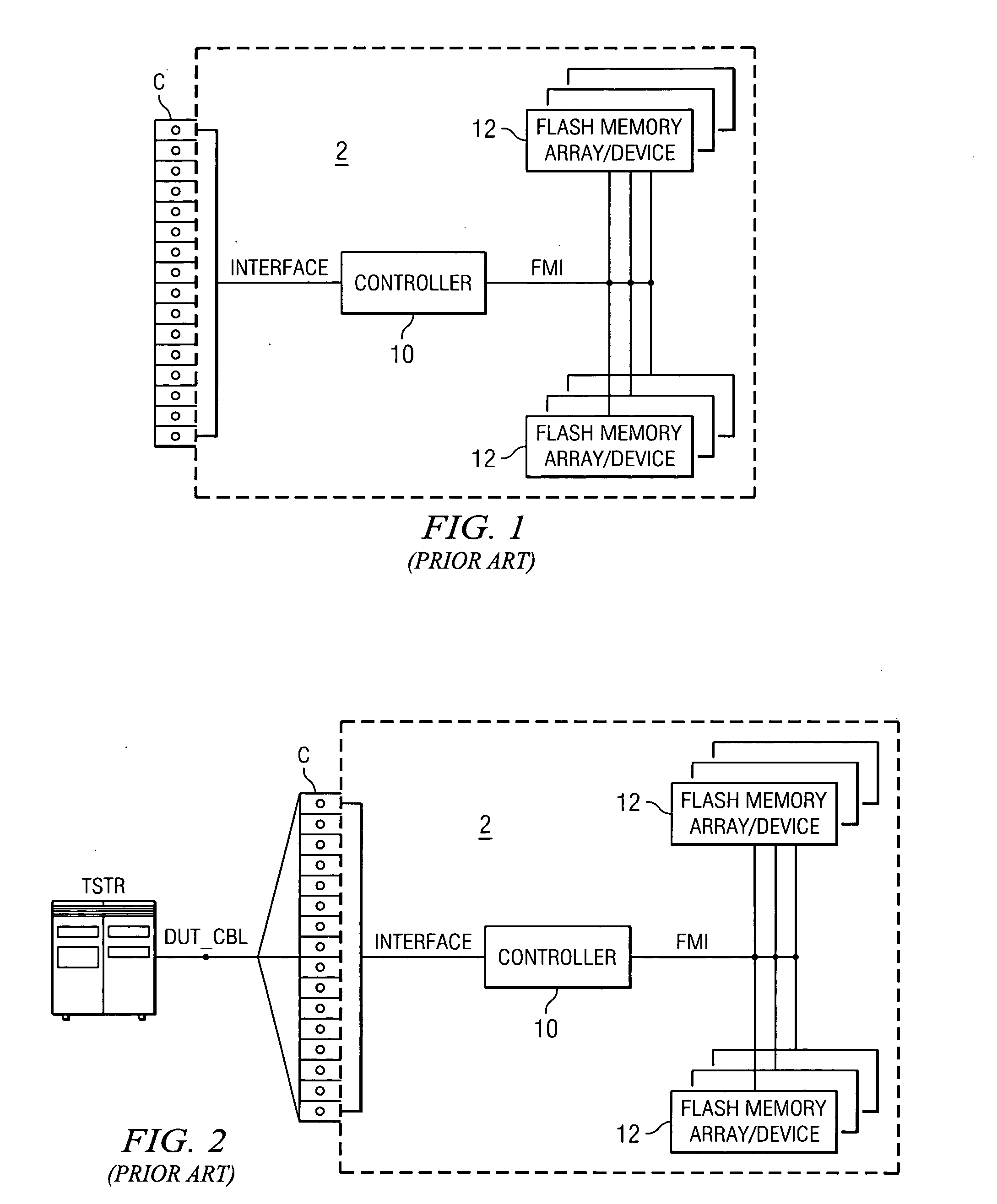
Unfortunately, conventional initialization methodologies cannot readily initialize flash memory 35 in this configuration, in which subsystem controller 29 is separated from flash memory and is embodied within SOC 20.
However, this conjectured approach requires the creation of special test hardware (tester TSTR and special bus SPC_BUS), as well as creation of the special interface into flash memory 35, both of which would add substantial cost to the manufacture and production of the system, and would limit the flexibility with which the system may be configured and initialized.

Method used


Image

  • Initialization of flash storage via an embedded controller
  • Initialization of flash storage via an embedded controller
  • Initialization of flash storage via an embedded controller

Examples


Embodiment Construction

[0026] The present invention will be described in connection with its preferred embodiment, namely as implemented into a system and method that utilizes test hardware to initialize flash memory for use by a system-on-a-chip (SOC) that includes the flash memory subsystem controller, such as a digital audio player (DAP). This particular exemplary implementation of the invention is selected because it is contemplated that this invention will be particularly beneficial when utilized in such an arrangement. However, it is also contemplated that the benefits of this invention may also apply to other architectures and implementations of flash memory systems. Accordingly, it is to be understood that the following description is provided by way of example only, and is not intended to limit the true scope of this invention as claimed.

[0027]FIG. 4 illustrates an exemplary implementation of the preferred embodiment of the invention, with reference to digital system 60. System 60 in this exampl...


PUM


Abstract

A digital system including flash memory, coupled to a system-on-a-chip within which a flash memory subsystem controller is embedded, is disclosed. The system-on-a-chip includes support for a standard external interface, such as a Universal Serial Bus (USB) or IEEE 1394 interface, to which a host system such as flash memory test equipment can connect. Initialization of the flash memory is effected by opening a communications channel between the host system and the embedded flash memory subsystem controller. The host system can then effect initialization of the flash memory subsystem, including formatting of the flash memory arrays, loading application programs, and the like, over the communications channel.

Description

CROSS-REFERENCE TO RELATED APPLICATIONS [0001] Not applicable. STATEMENT REGARDING FEDERALLY SPONSORED RESEARCH OR DEVELOPMENT [0002] Not applicable. BACKGROUND OF THE INVENTION [0003] This invention is in the field of flash memory systems, and is more specifically directed to the initialization of flash memory as used for integrated digital systems. [0004] The popularity of the non-volatile solid-state memory technology that is commonly referred to as “flash” memory has greatly increased in recent years. Flash memory typically refers to electrically-erasable semiconductor memory that can be erased and rewritten in relatively small blocks, rather than on a chip-wide basis, or in relatively large blocks as in conventional EEPROM devices. Flash memory has become especially popular for applications in which non-volatility (i.e., data retention after removal of power) of the stored data is essential, but in which the frequency of rewriting is relatively low. Examples of popular applicat...

Claims


Application Information

Patent Timeline
IPC IPC(8): G06F15/177
CPCG11C16/20G06F12/00G06F13/16G06F15/177G06F9/445
Inventor M. CONLEY, KEVIN
Owner SANDISK TECH LLC
Learn More